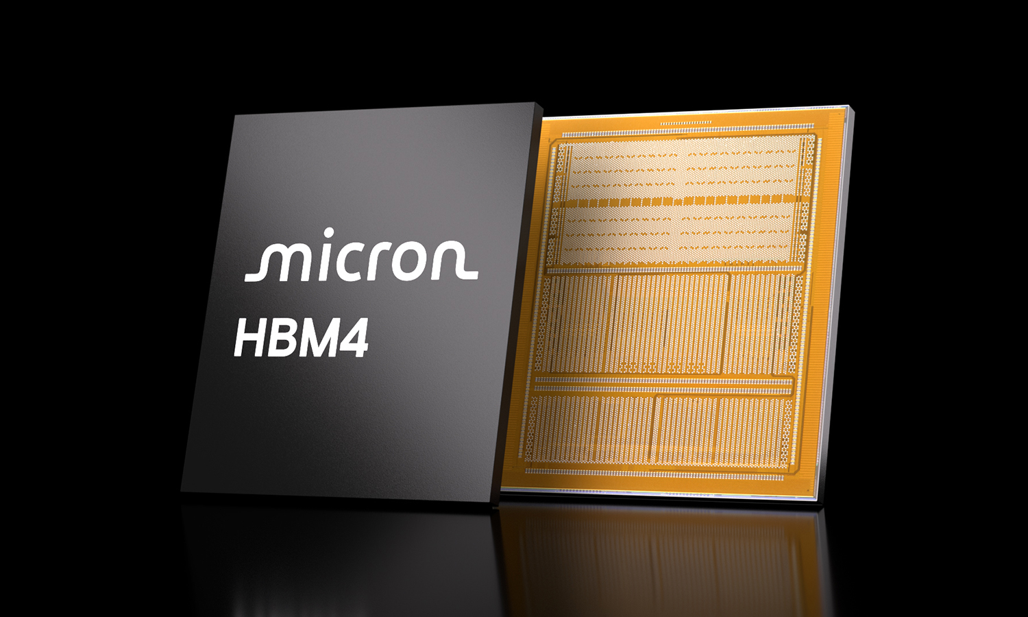
JEDEC Approves SPHBM4 Standard to Make HBM4-Class Memory More Affordable for AI and HPC Chips
The race for faster AI and high-performance computing hardware has pushed HBM memory into the spotlight. Today’s most advanced AI accelerators and HPC processors rely heavily on high-bandwidth memory to feed massive compute engines with data at extreme speeds. HBM4 is already becoming the foundation for next-generation chips, while enhanced versions are being evaluated by leading semiconductor companies.
However, there is a major problem: HBM is expensive, difficult to package, and increasingly hard to source in large volumes. As demand for AI servers continues to climb, premium DRAM supply remains tight, and HBM has become one of the biggest bottlenecks in the semiconductor industry.
That is where JEDEC’s newly approved SPHBM4 standard could become important.
SPHBM4, short for Standard Package HBM4, is designed to deliver HBM4-class bandwidth while reducing the need for costly advanced packaging. The goal is to keep much of the performance benefit of HBM4 while making high-bandwidth memory easier and cheaper to integrate into a wider range of chips.
Traditional HBM depends on complex packaging methods because it requires a large number of signal pins and very close placement near the compute die. These requirements help achieve massive bandwidth, but they also increase manufacturing cost, limit design flexibility, and add pressure to an already constrained supply chain.
SPHBM4 takes a different approach. Instead of relying on the same high pin-count structure as existing HBM4 designs, the new standard reduces the number of signal pins significantly. To compensate for that reduction, SPHBM4 increases signal speed by around four times. This allows the memory to maintain HBM-class bandwidth while cutting the signal pin requirement to roughly one-fifth of conventional HBM4.
In simpler terms, SPHBM4 aims to move the same amount of data through fewer physical connections by making each connection much faster.
This shift could have major benefits for AI accelerators, data center processors, and future HPC systems. By supporting standard packaging structures, SPHBM4 can reduce dependence on expensive advanced packaging technologies. That may help chipmakers lower production costs, improve scalability, and bring high-performance memory to more products beyond only the most expensive flagship AI hardware.
Another important change involves the distance between memory and the compute die. SPHBM4 allows a connection distance of around 20 mm, which is longer than traditional HBM layouts. This added spacing can improve internal thermal management, giving chip designers more flexibility when dealing with heat in large, power-hungry AI and HPC packages.
Thermals are becoming a critical issue as processors, GPUs, and AI accelerators continue to grow in size and power consumption. A memory standard that supports strong bandwidth while also allowing better heat distribution could make next-generation chip packages easier to design and cool.
SPHBM4 may also fit well with the industry’s growing interest in glass substrates. Glass substrates are being explored as a future foundation for large semiconductor packages because they offer advantages such as improved flatness, better thermal stability, and the ability to support finer wiring patterns compared with many existing substrate materials.
Although glass substrates are not yet in mass production, trial production is expected over the next few years, with broader commercialization likely closer to the end of the decade. If glass substrates become widely adopted, SPHBM4 could gain even more relevance by offering a more economical way to place HBM-class memory inside large chip packages.
The approval of SPHBM4 also reflects a broader trend in the memory industry. Companies are looking for alternatives that can ease the cost and supply challenges surrounding traditional HBM. Other concepts, including new stacked memory and flash-based approaches, have been discussed, but most have not yet reached commercial deployment. SPHBM4 stands out because it builds on the HBM4 ecosystem while changing the packaging and signal strategy to make it more practical for wider adoption.
For the AI industry, this could be a meaningful step forward. The demand for high-bandwidth memory is not slowing down. Training large AI models, running inference at scale, powering supercomputers, and supporting data-intensive workloads all require fast memory close to the processor. If memory supply remains limited and costs continue to rise, it could slow the rollout of next-generation computing systems.
SPHBM4 offers a potential path around that problem. By reducing pin count, supporting standard substrates, improving package flexibility, and maintaining high bandwidth, it could help make advanced memory more accessible across a broader range of hardware.
It is unlikely to replace premium HBM4 in every high-end design, especially where maximum performance is the only priority. But it could become an attractive option for systems that need HBM-like bandwidth without the full cost and complexity of traditional HBM packaging.
As AI hardware continues to evolve, memory technology is becoming just as important as raw compute power. Faster GPUs and accelerators are only useful if they can receive data quickly enough. JEDEC’s SPHBM4 standard is aimed directly at that challenge, offering a more cost-efficient way to deliver high-bandwidth memory performance for future AI, HPC, and data center platforms.
If adoption grows, SPHBM4 could help reduce pressure on the HBM supply chain, lower packaging costs, and open the door to more scalable AI systems in the years ahead.