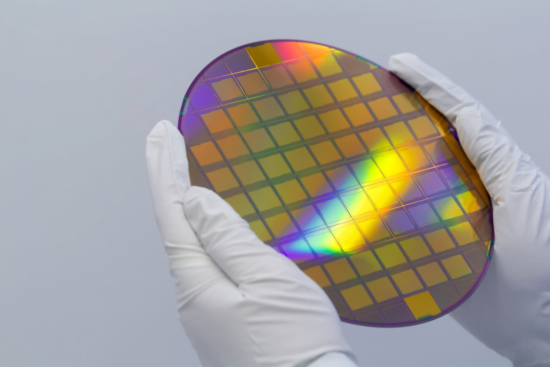
Samsung’s rocky 3nm chapter looks set to give way to a far more consequential leap: its first 2nm gate-all-around (GAA) lineup. The Exynos 2600 is expected to be the company’s first mobile SoC produced on this new architecture. But insiders say the real make-or-break moment arrives with Samsung’s second-generation 2nm process, known as SF2P, which will ultimately define whether the company can contend at the bleeding edge. With TSMC also preparing full-scale 2nm production, the race is tightening as the year winds down.
There’s already serious interest in Samsung’s 2nm roadmap. Reports indicate Samsung secured a multibillion-dollar deal with Tesla to fabricate chips on its 2nm GAA technology. The focus is Tesla’s AI6 silicon, designed to power the company’s next-generation Full Self-Driving system, robotics, and data-center workloads. According to ZDNet, SF2P is expected to enter mass production next year and deliver roughly a 12 percent performance uplift and about 25 percent better power efficiency compared to Samsung’s first-gen 2nm node. Samsung has completed SF2P’s basic design, signaling how aggressively it’s pushing to put its foundry business on equal footing with its chief rival.
The challenge, as always at this scale, is yield. While details on SF2P’s yields remain scarce, one industry insider characterizes the node as pivotal not just for Samsung’s foundry ambitions but also for its in-house Exynos roadmap. Yields have not yet stabilized, the source notes, but they are expected to improve meaningfully in the second half of the year as process work continues.
Samsung forecasts robust demand for 2nm wafers for up to four years and is already developing a third-generation 2nm process, SF2P+, with plans to implement it within about two years. If the company can execute on SF2P’s promises—higher performance, better efficiency, and competitive volume—its 2nm strategy could mark a turning point for both its mobile silicon and its broader foundry business.


