Huawei LogicFolding Faces Thermal Challenges as Qualcomm and Apple Stick With Advanced Chip Miniaturization
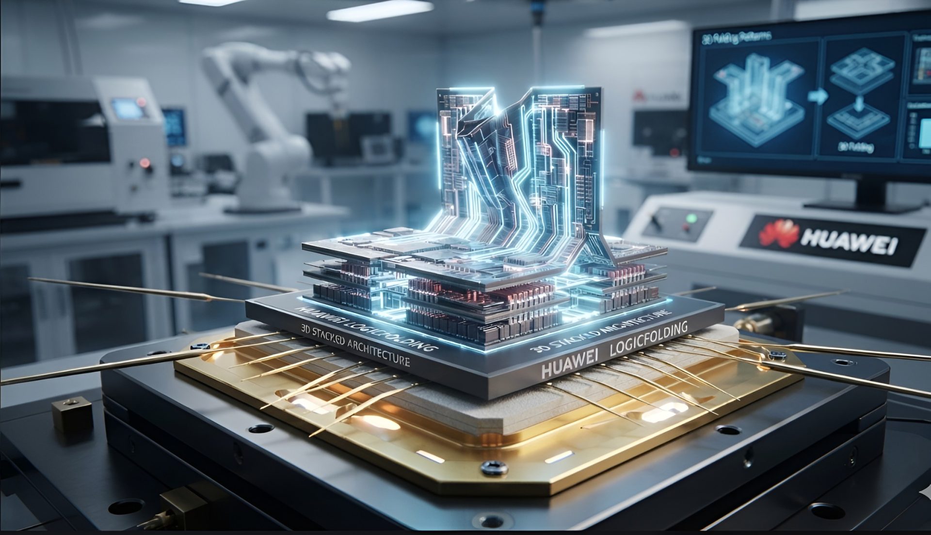
Huawei’s LogicFolding technology has attracted major attention in the semiconductor industry, especially as the company continues to develop alternatives amid ongoing restrictions on access to the most advanced chipmaking tools. The idea is ambitious: stack logic circuits vertically to improve compute density and shorten the distance signals must travel inside a chip.
However, while the technology is innovative, it may not be enough to challenge the mobile chip strategies used by Qualcomm and Apple. Both companies continue to rely heavily on leading-edge process miniaturization, where smaller transistor nodes deliver better performance, lower power consumption, and improved efficiency.
Recent die shots of Huawei’s Kirin 9050 Pro have given a closer look at how LogicFolding works. The chip reportedly uses a compute die and an SRAM die bonded together through dense copper-to-copper hybrid bonding. This structure allows active silicon layers to be stacked face-to-face, creating a more compact design with shorter vertical interconnects.
In theory, this can help Huawei increase compute density even if the individual circuits are not as advanced as those produced on cutting-edge nodes from major foundries. LogicFolding can reduce the length of some internal connections, potentially cutting signal travel distance and improving communication between chip layers.
Huawei’s argument is that this design can reduce some power costs. By replacing longer planar wires with shorter vertical connections, the company claims interconnect lengths can drop by around 20 percent on average, with some critical paths shrinking by as much as 70 percent. The shorter pathways may also reduce the need for clock buffers, lowering capacitance, voltage requirements, and overall power consumption.
But the biggest challenge remains heat.
A semiconductor expert recently argued that LogicFolding introduces a thermal burden that could limit clock speeds and reduce overall chip performance. Even if the stacked architecture improves signal routing, placing active layers on top of each other can make heat harder to dissipate. In mobile devices, where thin designs and limited cooling capacity are major constraints, this becomes a serious problem.
The expert compared the issue to the thermal challenges seen with backside power delivery network technology, where power routing is moved to the back of the wafer while data lines remain on the front. While such designs can improve efficiency and layout, they also introduce new heat management concerns.
According to this analysis, even if Huawei limits high-performance cell stacking or reduces power consumption through shorter routing, the chip may still suffer from weaker heat dissipation. In other words, the chip may generate less heat in some areas, but the stacked design can make it harder to move that heat away efficiently.
This is especially important for mobile processors. Smartphones and tablets require chips that can run fast without overheating, draining the battery, or requiring bulky cooling systems. If LogicFolding needs active cooling to perform at its best, that makes it far less attractive for mainstream mobile chip designs.
That helps explain why Qualcomm and Apple are unlikely to adopt a similar approach for their flagship mobile SoCs in the near future. Both companies prioritize performance-per-watt, sustained efficiency, and compact thermal profiles. For now, traditional node advancement through foundry partners remains the more practical route.
Interest in Huawei’s chip-stacking technology rose after reports surfaced about Qualcomm purchasing certain patents from Huawei. However, Qualcomm later clarified that its broader patent agreement with Huawei was not tied to LogicFolding. The company also pushed back against claims that it was effectively paying Huawei in a way connected to this technology.
The broader takeaway is that Huawei’s LogicFolding is a creative response to difficult circumstances. It may help the company narrow the gap in certain areas despite limited access to the world’s most advanced manufacturing processes. By stacking logic vertically and using fine-pitch hybrid bonding, Huawei can increase density and improve internal communication inside its chips.
Still, chip performance is not only about density. Thermal efficiency, sustained clock speeds, power consumption, manufacturing yield, and device integration all matter. LogicFolding may solve some design challenges, but it appears to create new ones in heat management.
For Huawei, the technology could become a valuable tool as it works to improve domestic chip capabilities. But for companies like Qualcomm and Apple, which already have access to highly advanced process nodes, the trade-offs may not be worth it.
Some analysts believe Huawei may need several more years before its chip technology can match the efficiency of leading-edge processes such as TSMC’s N3E. If that timeline proves accurate, LogicFolding may serve as a bridge technology rather than a complete replacement for advanced node manufacturing.
Huawei’s LogicFolding remains one of the more interesting developments in mobile semiconductor design. It shows how chipmakers can use packaging, stacking, and interconnect innovation to compensate for limitations in process technology. But unless the thermal challenges are solved, it is unlikely to become the preferred path for the world’s top mobile chip designers.