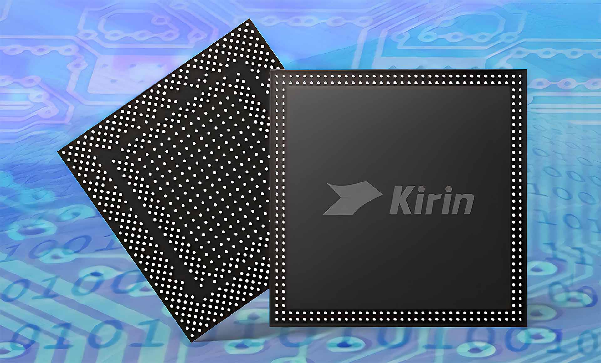
Huawei is gearing up to make a significant leap in the chip industry with the development of an advanced 3nm GAA node. This ambitious plan positions the Chinese tech giant to become a formidable competitor on the global stage.
Huawei has long been a trailblazer in China, not only in mobile technology but also in AI and computing, challenging Western counterparts with its innovative products. A recent report from Taiwan Economic Daily highlights Huawei’s research and development push towards the 3nm GAA node, following the successful launch of the Kirin X90 SoC built on a 5nm process provided by SMIC.
The company’s decision to adopt Gate-All-Around (GAA) technology for 3nm is noteworthy. By moving away from conventional silicon designs, Huawei plans to use “two-dimensional” materials for its transistor channels. This shift could enhance performance while reducing size and power consumption, a feat only attempted by Samsung Foundry at this scale. This raises intriguing possibilities for collaboration between Huawei and other industry leaders.
Additionally, Huawei is exploring a “carbon-based” 3nm design featuring carbon nanotubes, potentially offering an alternative to traditional silicon components. Partnering with China’s major foundry, SMIC, Huawei seems poised to revolutionize the approach to semiconductor fabrication.
Although these plans are in their nascent stages, Huawei’s track record in 5nm technology—successfully bringing it to consumer products—suggests substantial advancements ahead. As Huawei strengthens its position in the supply chain, it stands ready to challenge Western technology with homegrown innovations, promising a dynamic future for the global tech landscape.