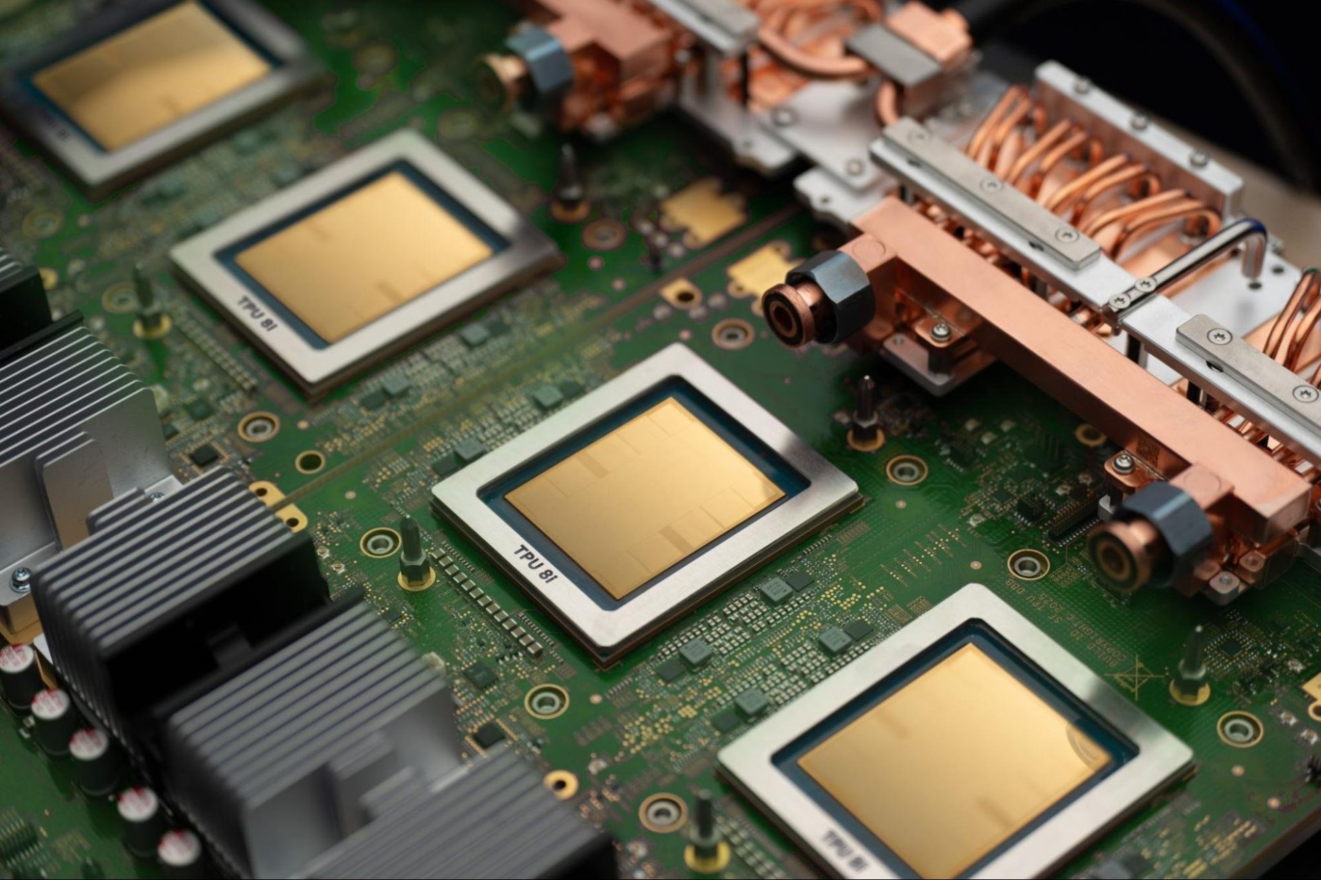
Google is reportedly exploring a major design shift for its next-generation Tensor Processing Unit, a move that could help the company reduce dependence on advanced chip-packaging technology while improving performance for its Gemini AI models.
As the artificial intelligence race accelerates, major technology companies are working to build custom AI chips that can serve as alternatives to NVIDIA’s high-demand GPUs. NVIDIA remains the dominant force in AI acceleration, but its chips are expensive and often difficult to secure in large quantities. That has pushed companies such as Google and Amazon to invest heavily in in-house silicon designed to lower costs, improve energy efficiency, and optimize AI workloads.
According to a report from Morgan Stanley, Google is developing a new TPU design known as “Frozen V2.” The chip is said to be built specifically for Gemini, Google’s family of AI models, and may take a different approach from current high-performance AI processors by placing SRAM memory directly on the silicon.
This design could reduce or even remove the need for advanced external packaging methods commonly used to connect memory and compute components in AI chips. In today’s AI hardware market, packaging technology plays a critical role because AI workloads require massive amounts of data to move quickly between processors and memory. However, these packaging methods can be costly, capacity-limited, and technically complex.
By integrating SRAM directly onto the chip, Google may be aiming to address one of the biggest challenges in AI computing: the memory-compute bottleneck. When data has to move between separate memory and processing units, performance can be limited and energy consumption can rise. Keeping memory closer to the compute engine can improve efficiency, lower latency, and help AI models run faster.
The reported Frozen V2 TPU appears to be part of Google’s broader strategy to build AI infrastructure that is tightly optimized for its own software. Rather than designing a general-purpose accelerator, Google could tailor the chip around the specific requirements of Gemini. This kind of hardware-software co-design may allow Google to improve performance per watt and reduce infrastructure costs across its AI services.
Morgan Stanley reportedly expects early production of Frozen V2 to begin in 2027, with a larger production ramp targeted for 2028. The report also suggests that Marvell could potentially be involved as a partner, though no official confirmation has been made.
The concept of hardwiring memory or AI-related data structures into silicon is not entirely new. Other AI chip developers have explored similar ideas to reduce the constant movement of data between memory and compute resources. This can lead to faster inference and more efficient processing, especially when a chip is built for a specific model or family of models.
However, this strategy comes with trade-offs. If a chip is deeply customized for one AI model, a major upgrade to that model could require a new chip design to achieve the same level of optimization. That means each significant model change may bring additional engineering work, manufacturing adjustments, and production complexity.
For Google, the potential benefits may outweigh the challenges. Gemini is a central part of the company’s AI ambitions, powering products across search, cloud services, productivity tools, Android, and other platforms. A dedicated TPU that can run Gemini more efficiently could give Google greater control over AI performance, cost, and scalability.
The move also reflects a wider shift in the AI chip industry. As AI models grow larger and more complex, companies are no longer relying only on standard GPU clusters. Instead, they are building custom accelerators, experimenting with new memory layouts, and searching for ways to reduce power consumption while increasing throughput.
If Google succeeds with Frozen V2, it could strengthen the company’s position in the custom AI chip market and reduce reliance on limited packaging capacity. More importantly, it could help Google run Gemini models at scale with better efficiency, which is becoming increasingly important as AI demand continues to rise.
While many details remain unconfirmed, the reported design points to an important trend: the next phase of AI hardware may be less about simply adding more compute power and more about rethinking how memory and processors work together. For companies building large AI systems, that could become the key to faster, cheaper, and more energy-efficient artificial intelligence.