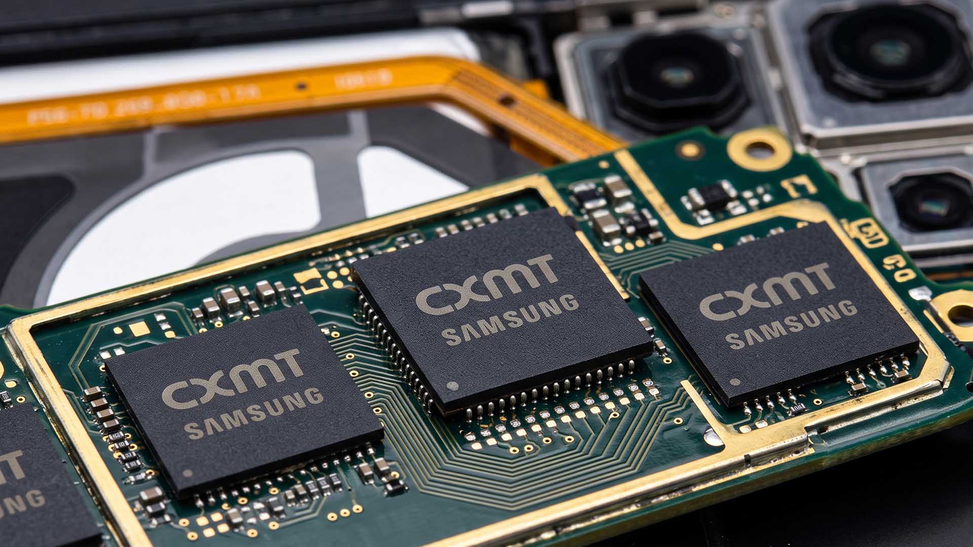
CXMT Advances Toward 1a DRAM With HKMG Technology and Major Capacity Expansion
CXMT appears to be making one of its most important advances yet in DRAM manufacturing, as the Chinese memory maker reportedly applies High-k Metal Gate technology to its DRAM transistors. This move could help reduce leakage current, improve power efficiency, and support the company’s transition toward more advanced process nodes, including 1a DRAM and beyond.
As DRAM technology continues to shrink, manufacturers face a serious challenge: traditional silicon dioxide insulation becomes less effective at extremely small scales. When the insulating layer gets too thin, electrical current can leak through it due to quantum tunneling. This leakage wastes power, generates extra heat, and limits how far DRAM chips can be scaled.
To address that problem, CXMT is reportedly adopting High-k Metal Gate, also known as HKMG. This technology replaces the older silicon-based insulating material with a high-k dielectric material such as hafnium oxide. In simple terms, “k” refers to the dielectric constant, or how well a material can act as an electrical insulator. Hafnium oxide has a much higher dielectric constant than silicon dioxide, allowing memory transistors to retain charge more effectively while supporting smaller chip designs.
HKMG also replaces the traditional polysilicon gate electrode with specialized metal gate stacks. This change helps eliminate a long-standing efficiency issue known as polysilicon depletion, where part of the gate becomes electrically ineffective. By removing this limitation, DRAM transistors can operate more efficiently and switch states faster.
This is especially important for DRAM because each memory chip contains billions of tiny cells. Each cell typically includes one transistor, which acts as a switch, and one capacitor, which stores electrical charge. Reducing transistor leakage improves data retention, lowers power consumption, and helps control heat output. Faster switching also supports improved performance, which is crucial for modern memory used in smartphones, PCs, servers, AI hardware, and high-performance computing systems.
CXMT is believed to be applying HKMG technology to its G4 DRAM manufacturing process, which is widely associated with the 1z node, as well as to LPDDR5X memory products. This suggests the company may be preparing to move toward the more advanced 1a DRAM node. The possibility becomes even stronger given that CXMT is already working on its next-generation 15nm G5 DRAM process.
The company is also making progress in high-bandwidth memory. CXMT is reportedly in the risk-production stage for HBM2E using its 18nm G3 DRAM process. HBM2E is the third generation of high-bandwidth memory and is used in applications that require fast data transfer and high memory bandwidth. CXMT is also said to be sampling HBM3 on its G4 process, signaling growing ambitions in advanced memory markets tied to AI accelerators, data centers, and graphics processors.
In another important development, CXMT’s DDR6 memory chips have reportedly completed the research and development verification stage. That puts the technology one step closer to eventual mass production, though commercial availability will still depend on manufacturing readiness, yield improvements, and broader platform support.
Meanwhile, the world’s leading memory producers are pushing ahead with next-generation DRAM roadmaps of their own. Major competitors are moving toward sub-10nm-class D0a nodes while also exploring 3D DRAM and 4F² memory cell architecture. These future designs aim to stack parts of the memory cell vertically rather than spreading them horizontally, reducing the surface area required for each cell.
In a 4F² design, the footprint of a memory cell is reduced to a square measuring four times the minimum feature size squared. This structure uses bitlines and wordlines, which are the tiny interconnects that help control and access transistors inside each memory cell. If successfully commercialized, this type of architecture could allow memory makers to continue scaling DRAM even as traditional two-dimensional layouts become harder to shrink.
Alongside its technology progress, CXMT is rapidly expanding production capacity. The company is reportedly aiming to increase output to around 300,000 wafers per month by the end of this year, up from roughly 200,000 wafers per month currently. It is also expected to build dedicated high-bandwidth memory capacity of around 50,000 wafers per month.
CXMT’s expansion plans do not stop there. The company is building two new fabrication facilities in Shanghai and Hefei, which could eventually raise total production capacity to about 600,000 wafers per month. If this growth continues as expected, CXMT could become one of the largest DRAM manufacturers by volume over the next several years.
Longer-term projections suggest CXMT may add roughly 100,000 wafers per month in capacity every year from 2026 through 2031. By that point, the company’s total capacity could reach as high as 800,000 wafers per month.
The combination of HKMG adoption, progress in LPDDR5X, HBM, and DDR6, and rapid fab expansion shows that CXMT is working aggressively to strengthen its position in the global DRAM market. While the company still faces major challenges in yield, advanced manufacturing, equipment access, and competition from established memory leaders, its recent progress suggests it is moving quickly toward more advanced DRAM process technologies.
If CXMT successfully transitions from 1z to 1a DRAM and scales production efficiently, it could become a much more influential force in the memory industry, especially as demand continues to grow for AI servers, mobile devices, cloud infrastructure, and next-generation computing platforms.