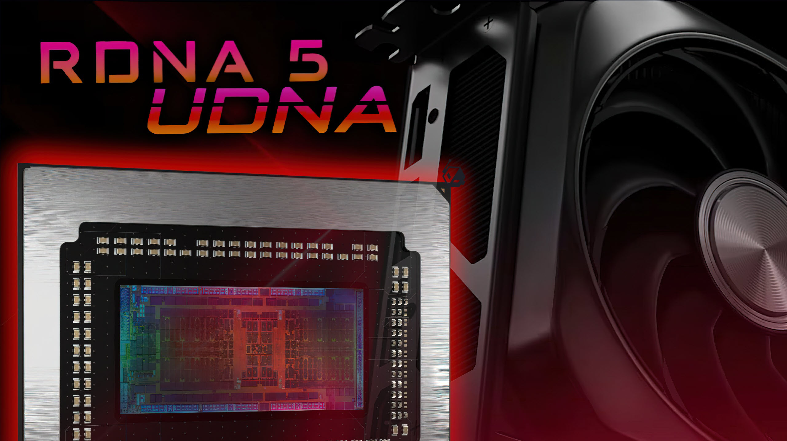
AMD’s next graphics architecture is starting to take shape, and if the latest rumor mill is on point, RDNA 5—also referred to as UDNA—could span four distinct dies with the flagship topping out at 96 compute units. The details come from new block diagrams shared by Kepler_L2 on enthusiast forums, adding more color to earlier speculation and reinforcing the idea that AMD is building a highly modular family this time around.
At the high end, the rumored top die is arranged into 8 Shader Arrays, each split into two Shader Engines, for a total of 16 Shader Engines. With 6 CUs per Shader Engine, that configuration lands at 96 CUs. Each Shader Engine is paired with its own Render Backend, all wired into a central SoC complex housing the Graphics Command Processor, Graphics Engine, hardware schedulers, and L2 cache. Memory is said to be handled by 16 controllers at 32 bits each, enabling up to a 512-bit bus. If AMD keeps its current Infinity Cache strategy, expect up to 128 MB on this die.
A step down, a 40 CU part is outlined with 4 Shader Arrays and 8 Shader Engines, again at 6 CUs per engine. This design reportedly carries six memory controllers for a 192-bit interface and as much as 48 MB of Infinity Cache. The diagrams hint that RDNA 5’s modular SoC approach—teased publicly at Hot Chips—will allow AMD to scale features cleanly across multiple SKUs off a common blueprint.
Entry-oriented chips are said to scale between 24 CUs and 12 CUs. The 24 CU die uses four Shader Engines/Arrays with 6 CUs each and eight memory controllers. Depending on controller width, that could translate to either a 128-bit or 256-bit bus, though a 256-bit pipe on this tier seems unlikely if the 40 CU model tops out at 192-bit. The smallest die features two Shader Engines/Arrays with 6 CUs total per side, adding up to 12 CUs. It’s paired with four memory controllers, which could yield either a 64-bit or 128-bit bus. On-cache sizing, the smaller chips are rumored to include around 32 MB and 16 MB of Infinity Cache, respectively.
There’s also chatter about bigger local caches per CU. On the datacenter side, AMD’s CDNA 5 architecture for MI400 reportedly jumps from the CDNA 4 combo of 32 KB L0 plus 160 KB LDS to a shared 448 KB L0/LDS. While that’s a different product class, UDNA is rumored to bring Radeon and Instinct designs closer together, opening the door for some of those cache learnings to flow into consumer GPUs.
All of this remains unconfirmed, so keep expectations in check. The next wave of AMD gaming GPUs is rumored to hit mass production around the second quarter of 2026. That timeline would set up a lively start to the year for PC graphics, with rival lineups expected to be jostling for attention around the same window.
Quick look at the rumored tiers:
– Flagship-tier: up to 96 CUs, 512–384-bit bus, 24–32 GB VRAM potential
– Mid-tier: around 40 CUs, 384–192-bit bus, 12–24 GB VRAM potential
– Low-tier: around 24 CUs, 256–128-bit bus, 8–16 GB VRAM potential
– Entry-tier: around 12 CUs, 128–64-bit bus, 8–16 GB VRAM potential
Which upcoming GPUs are you most excited to see, and where do you think AMD’s UDNA lineup will land on performance per watt and price?