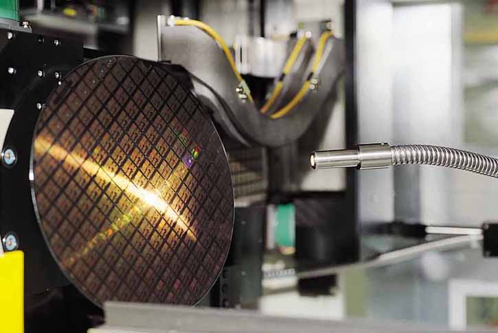
TSMC, the prominent Taiwanese semiconductor manufacturer, is on the verge of a technological breakthrough with the steady progress of its 2nm process technology. Boasting significant advancements, this future node is poised to redefine semiconductor performance benchmarks. The company has recently achieved notable yield-rate targets, indicating its readiness for mass production by 2025. This milestone assures that TSMC’s process is not only following the scheduled timeline but is also meeting the performance criteria needed for widespread adoption.
The 2nm process node, utilizing cutting-edge Gate-All-Around (GAA) technology, is garnering attention for its potential to provide substantial performance enhancements in semiconductor chips. Apple, Intel, and other tech titans have shown a keen interest in incorporating TSMC’s 2nm process into their upcoming products. This development holds significant implications for the industry, particularly with Apple’s Chief Operating Officer’s recent visit to Taiwan to secure future chip supplies.
The initial deployment of TSMC’s 2nm technology is expected to be seen in Apple’s M5 chips, designed for future Mac and iPad product lines, as well as in the A19 processor predicted to feature in the iPhone 17 series. Moreover, Intel’s roadmap hints at the integration of the 2nm process in their upcoming Nova Lake CPU lineup, underscoring a broader industry embrace of the technology.
TSMC announced that the yield for the 2nm 256 Mb SRAM device is hitting 80% success rates, a significant achievement demonstrating the node’s viability for mass production. Yield refers to the proportion of functional chips produced during the manufacturing process, and high yield rates are critical for the cost-effective adoption of new technologies. The GAA methodology has proven its worth by reaching 90% of its target performance goals, showing positive signs for the future of semiconductor manufacturing.
While TSMC appears to be leading the race with its 2nm process, competitors like Samsung have yet to announce updates on their comparable products. The industry will be closely monitoring the progress as these developments could signify a shift in the competitive landscape.
In the coming years, as TSMC’s 2nm process enters mass adoption, consumers can anticipate a wave of high-performance, energy-efficient devices transforming both professional and personal technology spaces. This progress represents not only a milestone for TSMC but also a leap forward for the entire semiconductor industry, promising an exciting future of technological innovation.