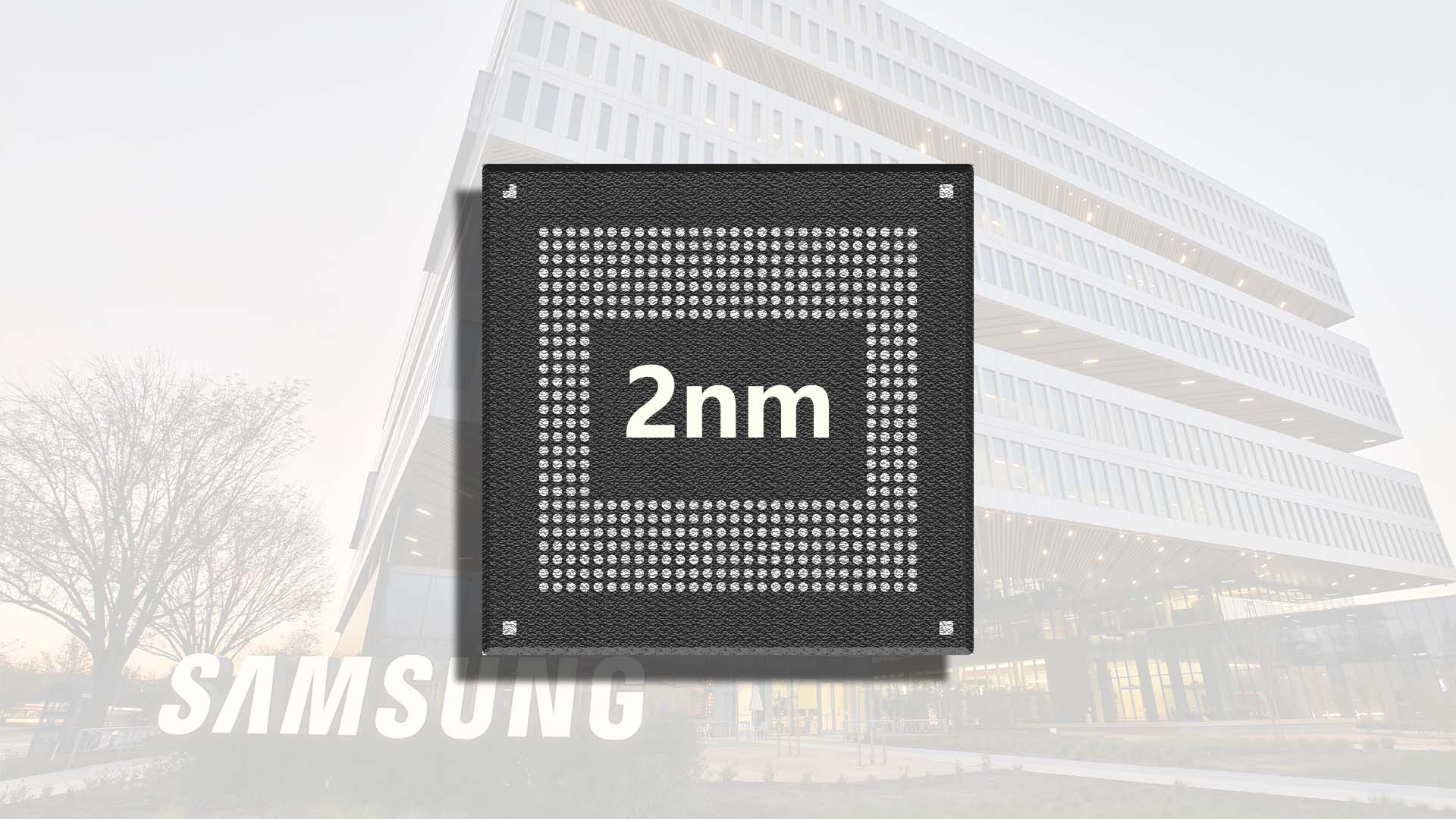
Samsung’s 2nm gate-all-around (GAA) era is no longer a blueprint—it’s on the factory floor. Mass production of 2nm GAA wafers began in late September, with the first chips slated for the upcoming Exynos 2600. Momentum appears strong enough for a wider rollout, and recent remarks from top executives in a high-level government meeting suggest the company is hitting key milestones faster than expected.
One of the biggest signals: the 2nm GAA yield target has reportedly been raised to 70 percent by year’s end, up from an earlier 50 percent goal. In chip manufacturing, higher yields translate directly to better economics, faster scaling, and more predictable delivery for customers—critical advantages as competition intensifies.
At a meeting chaired by Policy Chief Kim Yong-beom, the president and CTO of the Device Solutions Division, Song Jae-hyuk, outlined robust progress and a clear ambition to reclaim leadership in the global foundry market with this node. According to local reports, Samsung has already wrapped the basic design of its second-generation 2nm GAA process, while a third-generation iteration—referred to as SF2P+—is on track to complete development within about two years. The roadmap points to rapid refinement in performance, power efficiency, and density as the node matures.
The industry is taking notice. SK hynix Corporate President Song Hyun-jong called 2nm GAA a pivotal inflection point for semiconductors, while also underscoring the challenges of catching up with rivals, the need to deepen specialized talent, and the importance of government support to sustain momentum across the ecosystem.
As for real-world silicon, early internal testing of the Exynos 2600 suggests strong performance, with preliminary results indicating it can outpace rival flagship chips such as the A19 Pro and Snapdragon 8 Elite Gen 5 in a range of benchmarks. It’s worth remembering that internal numbers often differ from what ships in commercial devices, but the signs are promising for both performance and efficiency—key benefits expected from a mature GAA design at 2nm.
What this means for the market:
– Faster ramp to volume: Raising the yield target to 70 percent suggests manufacturing is stabilizing and scaling.
– Competitive roadmap: Second- and third-generation 2nm GAA designs indicate sustained investment in performance-per-watt and density.
– Ecosystem tailwinds: Strong foundry progress, coupled with support for talent and R&D, could accelerate innovation across mobile, AI, and high-performance computing.
– A flagship showcase: The Exynos 2600 looks set to be the first proof point for 2nm GAA in consumer devices.
Taken together, the yield improvements, aggressive roadmap, and encouraging early silicon paint a picture of a foundry that’s turning the corner. With full-scale 2nm chip production approaching, recent executive comments point to steady progress on both yield and performance targets—exactly what customers want to hear as the industry enters the next node transition.


