TSMC 2nm Production Reportedly Reaches 20,000 Wafers Per Month as Apple, Google and AI Demand Rise
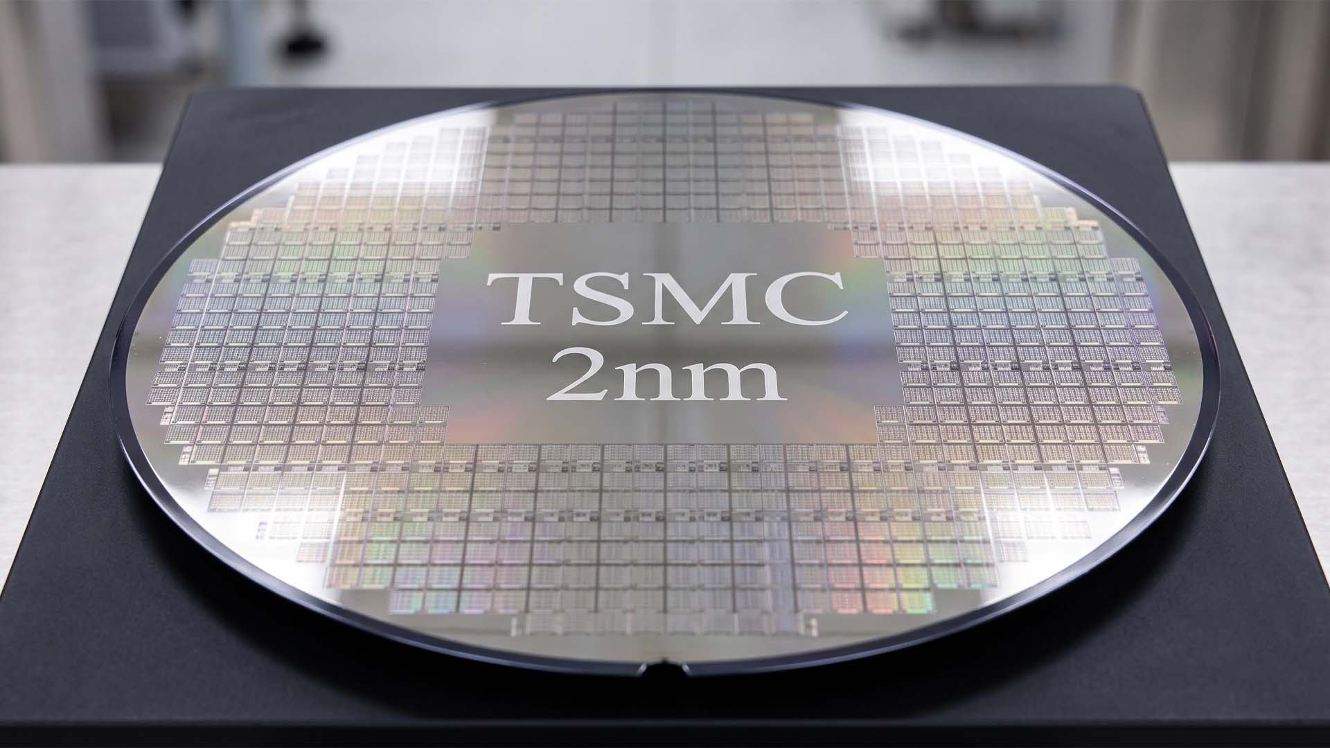
TSMC has reportedly reached an important production milestone as it pushes forward with its next major chip manufacturing upgrade. The semiconductor giant is said to have achieved 20,000 monthly wafers at one of its Taiwan facilities dedicated to 2nm chip production, marking a key step in the company’s transition from its current 3nm process to the more advanced 2nm node.
The milestone is especially significant because TSMC remains the world’s leading contract chipmaker, supplying advanced processors for smartphones, data centers, artificial intelligence hardware, and high-performance computing products. As demand for faster and more power-efficient chips continues to grow, the 2nm process is expected to become one of the company’s most important technologies over the next several years.
According to the report, five fabs in Taiwan are focused on 2nm production. Among them, Fab 20 has now reached the 20,000-wafers-per-month level. This indicates that TSMC is moving quickly to prepare capacity for major customers that are expected to adopt the new manufacturing process.
Even before customers have officially launched products using TSMC’s 2nm technology, the node has already begun contributing to the company’s revenue. The advanced process reportedly accounted for 3 percent of TSMC’s Q3 2026 revenue, showing that early production activity is already becoming commercially meaningful.
The company has also indicated strong interest in the 2nm node. During a previous earnings call, TSMC said its 2nm process had four times as many tape-outs compared with its 3nm process at a similar stage. Tape-outs are an important industry signal because they show how many chip designs are being prepared for manufacturing. A higher number suggests stronger customer demand and wider adoption potential.
Apple and Google are expected to be among the first major companies to introduce consumer products powered by 2nm chips. Google’s Pixel 11 series is likely to feature the Tensor G6 when the lineup is unveiled in August, while Apple is expected to follow with the A20 Pro chip for the iPhone 18 series in September.
While smartphones may help introduce 2nm technology to mainstream consumers, artificial intelligence customers are expected to drive much of the long-term wafer demand. AI accelerators and high-performance GPUs require enormous computing power, and moving to a more advanced node can help improve performance, efficiency, and transistor density.
For now, TSMC’s 3nm process still leads in total wafer output. The 3nm node reportedly produces around 175,000 wafers per month, reflecting continued demand from current-generation flagship chips and advanced computing products. However, as more customers shift future designs to 2nm, that balance is expected to change.
Major AI chip companies are already preparing products based on TSMC’s newest technology. AMD has confirmed that its MI455X GPU, designed for agentic AI workloads, will use TSMC’s 2nm process. NVIDIA is also expected to compete in the same space with its upcoming Rubin platform.
The move to 2nm is more than just another manufacturing upgrade. For TSMC, it represents a major opportunity to strengthen its leadership in advanced semiconductors at a time when AI, smartphones, and cloud computing are pushing chip performance requirements higher than ever.
If production continues to scale smoothly, TSMC’s 2nm process could become the company’s next major growth engine, following the success of its 3nm technology. With Apple, Google, AMD, NVIDIA, and other major customers expected to rely on advanced nodes for future products, demand for 2nm wafers may rise sharply in the coming years.