TSMC is accelerating the next big leap in chipmaking, pulling its 2-nanometer production plans forward and expanding aggressively in the United States to meet surging demand for AI and premium mobile devices. The company now targets volume production of its N2 process in 2025, with a wider ramp in 2026—several years earlier than the previously floated 2030 timeframe. Early yields are said to be promising, and an enhanced N2P variant is already on the roadmap for late 2026.
The move follows a standout quarter that underscores how AI is reshaping the semiconductor industry. In Q3 2025, TSMC reported $33.1 billion in revenue, up more than 40 percent year over year, fueled by large orders tied to data center AI accelerators and high-end smartphones from customers such as Nvidia and Apple. To sustain momentum, the company plans to invest $42 billion in 2025 to expand capacity in Taiwan and abroad.
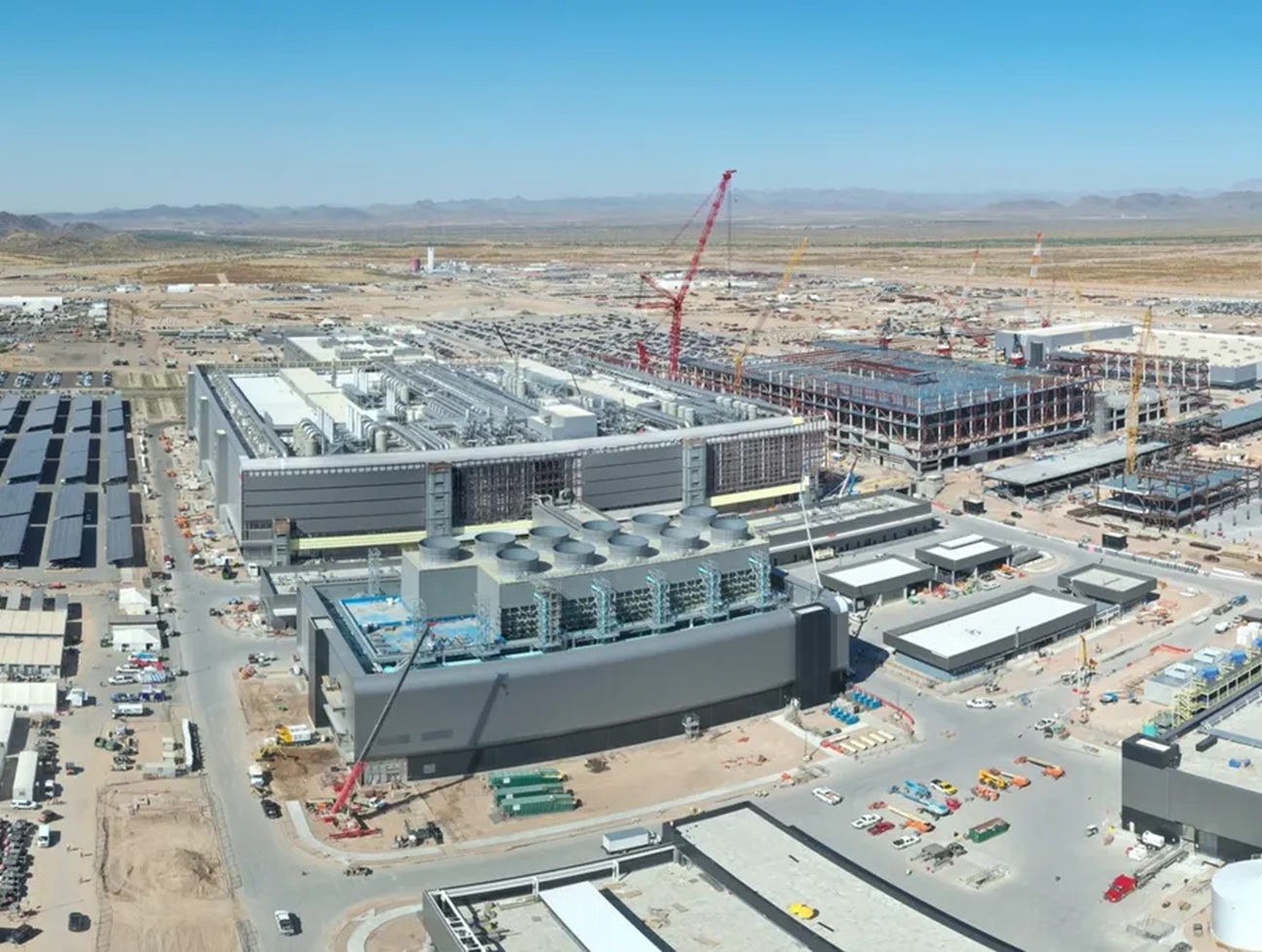
A centerpiece of that expansion is the fast-evolving Arizona campus. Originally planned for 3 nm and 4 nm, the complex is being upgraded to support 2 nm manufacturing and prepared to accommodate future A16-class products. If the current roadmap holds, the site could become one of the most advanced semiconductor hubs outside Asia, potentially accounting for around 30 percent of the company’s next-generation output. Target capacity from Arizona is projected at roughly 100,000 wafers per month once fully ramped. To support that scale, TSMC is building out on-site packaging and testing, developing a broader local supplier ecosystem, and evaluating additional land acquisitions.
Why this matters:
– The accelerated N2 and N2P timeline positions TSMC at the forefront of high-performance, energy-efficient chips that power AI training, inference, and top-tier mobile devices.
– A major 2 nm footprint in the United States aligns with policy goals to boost domestic chip production and reduce reliance on overseas foundries.
– Expanded advanced-node capacity helps ease supply constraints as AI workloads explode and smartphone makers push for more efficient, more powerful silicon.
What to watch next:
– The pace of N2 yield improvements and the speed of the 2026 ramp.
– How quickly the Arizona site reaches its targeted wafer output and integrates advanced packaging at scale.
– Customer adoption across AI accelerators, flagship smartphones, and other high-performance computing segments as N2 and N2P come online.
Bottom line: With earlier 2 nm production, record demand from AI and premium mobile, and a rapidly maturing US fab network, TSMC is tightening its grip on next-generation semiconductor leadership and reshaping the global supply chain in the process.


