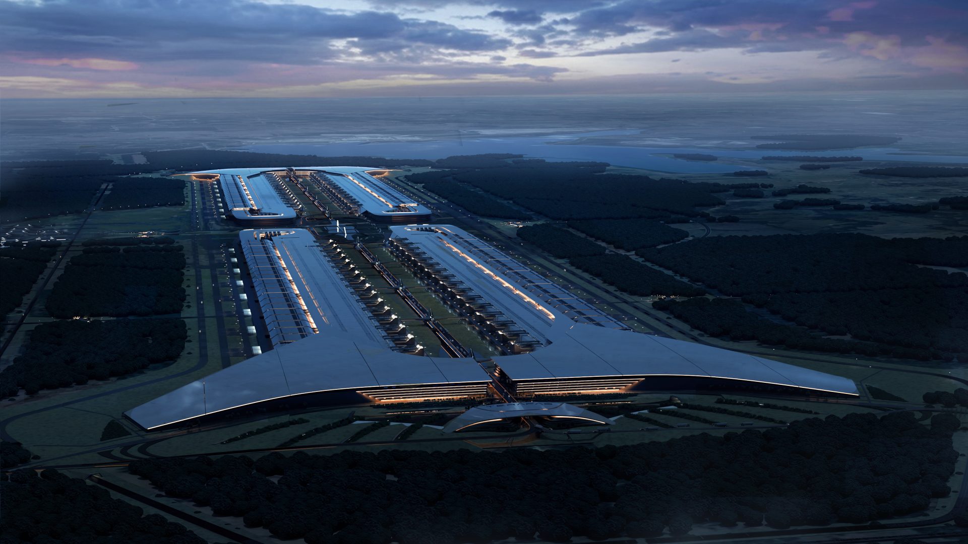
Elon Musk’s Terafab Targets Massive Chip Production for Tesla, SpaceX, and AI Compute
Terafab, the reported semiconductor joint venture tied to Tesla and SpaceX, is shaping up to be one of Elon Musk’s most ambitious infrastructure projects yet. The goal is not simply to build another chip factory, but to create a deeply integrated semiconductor ecosystem capable of supporting future AI, robotics, and space-based computing needs at an enormous scale.
According to recent supply chain reports, Terafab has informed semiconductor equipment suppliers that it is targeting production capacity of around 1 million wafers per month by 2032. If achieved, that would place the project among the most significant chip manufacturing efforts in the world.
The planned output is reportedly split between 700,000 wafers per month for memory chips and 300,000 wafers per month for logic chips. That balance highlights what Terafab appears to be built for: powering high-performance AI systems that require both advanced processing and vast amounts of memory bandwidth.
For Tesla, that could mean a more reliable supply of chips for its Optimus humanoid robots, self-driving systems, and AI training infrastructure. For SpaceX, the same manufacturing base could support next-generation satellites, space-based data centers, and advanced computing systems designed for off-world or orbital operations.
The scale of the project is striking. Samsung’s current DRAM production capacity is estimated to be in the range of 650,000 to 700,000 wafers per month. Terafab reportedly wants to reach a similar memory production level within roughly six years, despite being a new entrant in one of the most technically demanding industries on the planet.
Terafab is still in its early stages, but the project is already associated with a planned $16.8 billion semiconductor complex in Grimes County, Texas. Over time, the site could reportedly expand to cover up to 100 million square feet, making it one of the largest chip manufacturing campuses ever proposed.
The broader vision behind Terafab appears to be vertical integration. Instead of relying on a fragmented global supply chain for chip design, manufacturing, packaging, and testing, the project aims to bring many of these processes under one roof. That could include mask generation, lithography, advanced chiplet packaging, and final testing.
If successful, this approach could dramatically shorten chip development cycles. Today, advanced semiconductor design and manufacturing loops can take six to nine months. Terafab’s model reportedly aims to reduce that timeline to just weeks, giving Tesla and SpaceX far greater control over hardware iteration.
That speed could be especially important for AI. As companies race to build more powerful models, more efficient inference systems, and specialized chips for robotics, the ability to rapidly design and produce custom silicon may become a major competitive advantage.
The project is also expected to use Intel’s 14A process for logic chips, suggesting that Terafab may combine in-house manufacturing ambitions with outside process technology support. This could help the venture move faster while still working toward long-term control over its chip supply.
There are also reports that Terafab is renegotiating potential partnership terms with TSMC. Key issues are said to include operational control and investment commitments. Musk has previously suggested that he does not want the Taiwanese chipmaker to own or run Terafab, indicating that control over manufacturing strategy remains a major priority.
The motivation is clear: Tesla and SpaceX are increasingly dependent on advanced compute. Tesla needs chips for autonomous driving, robotics, AI training, and future mobility platforms. SpaceX may require powerful, efficient processors for satellites, communications networks, and potential space-based data centers. A dedicated semiconductor operation could reduce dependency on outside suppliers and help secure long-term chip availability.
Still, the challenges are enormous. Semiconductor manufacturing is one of the most capital-intensive and technically complex industries in the world. Building a facility is only the beginning. Terafab would need leading-edge equipment, a highly skilled workforce, reliable materials supply, strong yield rates, and the ability to compete with companies that have decades of manufacturing experience.
Even so, the reported 1 million wafers-per-month target shows the level of ambition behind the project. Terafab is not being positioned as a small experimental fab. It is being framed as a strategic manufacturing powerhouse designed to support the AI-driven future of Tesla, SpaceX, and Musk’s broader technology ecosystem.
If the project reaches its goals, Terafab could become a major force in semiconductor manufacturing by the early 2030s. More importantly, it could give Tesla and SpaceX something few technology companies possess: direct access to large-scale chip production tailored specifically to their own hardware, AI, robotics, and space computing needs.