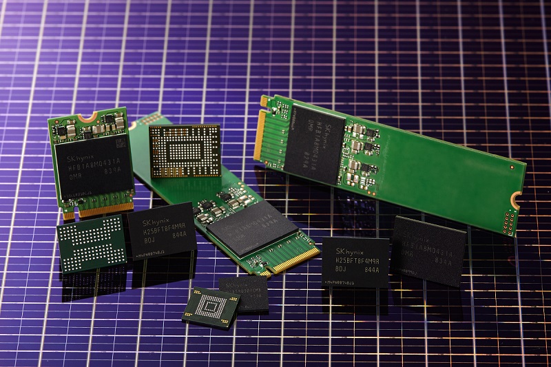
SK Hynix is setting its sights on new heights in storage technology with plans to produce a groundbreaking 400-layer NAND flash memory by the end of 2025. This ambitious target follows the successful demonstration of their 321-layer NAND in August 2023 and plans to commence mass production of this innovative flash memory in the first half of 2025.
The drive to increase storage capacity is an ongoing challenge within the tech industry, and SK Hynix is leading the charge with their forward-looking storage solutions. To produce such high-capacity NAND, the company is engaging with numerous cutting-edge technologies, focusing on new materials and methods for hybrid bonding. These enable the binding of different wafers through sophisticated processes like polishing, etching, deposition, and wiring.
The comprehensive process of creating multilayer NAND involves meticulous cell structure design, arranging the cells in each layer perfectly, and methodically aligning them during the stacking process. This requires the silicon wafers to be scrupulously cleaned and layered with thin films of SiO2 and Si3N4. The precision required in such a repeated layering process is immense, demanding painstaking attention to detail to achieve the desired outcome.
As SK Hynix gears up for production of its 321-layer NAND, competition within the industry is fierce. Memory heavyweights such as Samsung and Micron are already pushing the envelope with their respective 290-layer and 276-layer NAND chips. In addition, Samsung has set an ambitious goal to surpass 1000 layers by 2030, while Japanese firm Kioxia is also marching towards a 1000-layer milestone with its current 218-layer 3D NAND.
SK Hynix’s strategy to reach 400 layers involves the Peripheral Under Cell method, where memory cells are efficiently stacked above peripheral circuits. This clever configuration, however, requires some innovative solutions to prevent damage to the peripheral circuits from the heat and pressure of additional layers. One proposed solution is hybrid bonding, a technique in which memory cells and peripheral circuits are developed on separate wafers and then fused together.
This advanced form of bonding minimizes the risk of damage while maintaining the compactness necessary for today’s slim, high-capacity devices. The use of high layer count NAND chips has the exciting potential to exponentially increase data storage without needing larger chips, creating cost-effective and space-saving opportunities for consumers and businesses alike.
As the industry watches for SK Hynix’s progress towards its 400-layer NAND, the potential impact on the market is significant. The realization of such technology would not only redefine the landscape of data storage capacity but also potentially usher in a new era of affordable, high-performance memory solutions.