SK Hynix Expands U.S. Engineering Push for 3D Stacked DRAM and On-Device AI
SK Hynix is strengthening its presence in the United States as it moves deeper into the next generation of memory technology. The company is recruiting engineers in San Jose to help develop 3D stacked DRAM-on-logic solutions in collaboration with American customers, signaling a major step beyond its current focus on high-bandwidth memory.
The move highlights how quickly the memory industry is changing. As artificial intelligence workloads shift from massive cloud data centers to smartphones, PCs, vehicles, wearables, and edge devices, demand is rising for memory systems that are faster, more efficient, and more tightly integrated with processors. SK Hynix appears to be positioning itself at the center of that transformation.
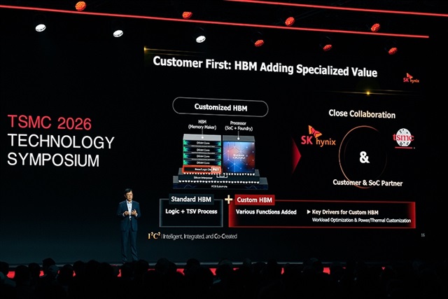
At the TSMC Technology Symposium 2026, SK Hynix Chief Development Officer Ahn Hyun discussed the importance of memory-logic integration, a concept that could become critical for future AI devices. Traditional memory and logic chips are usually separated, which can create bottlenecks when large amounts of data need to move quickly between computing and storage components. By stacking DRAM directly with logic, chipmakers can reduce latency, improve power efficiency, and increase performance in compact devices.
This strategy builds on SK Hynix’s success in high-bandwidth memory, which has become essential for AI accelerators and advanced data center hardware. However, the company’s latest direction suggests it does not want to rely only on HBM growth. Instead, it is expanding into custom memory solutions designed for specific customer needs and new AI-driven use cases.
The San Jose hiring effort is especially important because it places SK Hynix engineers closer to major U.S. technology companies working on AI chips, consumer electronics, autonomous systems, and next-generation computing platforms. Co-designing memory with customers can help create more optimized products, allowing memory and logic architecture to be developed together rather than treated as separate parts of a system.
For on-device AI, this kind of integration could be a key advantage. Running AI tasks locally requires chips that can process data quickly without consuming too much power. Whether the device is a smartphone using generative AI features, a laptop handling real-time translation, or a car processing sensor data, efficient memory access is one of the biggest challenges. 3D stacked DRAM-on-logic could help address that challenge by bringing memory closer to the compute engine.
SK Hynix’s recruitment push also reflects a broader industry trend: memory companies are no longer just supplying standardized components. They are becoming strategic partners in chip design, particularly as AI hardware becomes more specialized. Custom memory architecture is expected to play a larger role in improving performance, reducing energy use, and enabling new device categories.
By investing in U.S.-based engineering talent, SK Hynix is sending a clear message that it wants to be more involved in early-stage product development with key customers. The company’s focus on 3D stacked DRAM, memory-logic integration, and AI-ready memory solutions could help shape the future of both cloud and edge computing.
As AI continues to spread across everyday devices, the need for smarter memory design will only grow. SK Hynix’s latest move suggests that the next major leap in AI performance may not come from processors alone, but from a closer partnership between memory and logic.