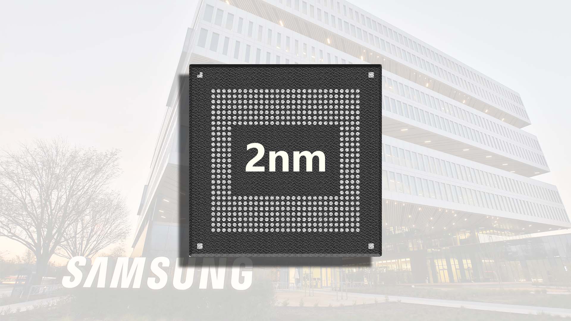
Samsung’s ambitious journey into cutting-edge semiconductor technology has faced some bumps along the way, with their highly anticipated 1.4nm process experiencing delays. However, this isn’t a setback for the tech giant. Instead, Samsung plans to fast-track its third-generation 2nm process within two years, offering significant enhancements over its predecessor.
At a recent SAFE forum, Samsung showcased its advanced 2nm technology. This innovation, dubbed SF2P+, utilizes an Optic Shrink technique to enhance the company’s second-generation 2nm node. The result? A notable 20-30% performance increase over current technologies.
Rather than rushing to the next big thing, Samsung aims to refine its existing processes to stabilize yields and enhance competitiveness, particularly against formidable rival TSMC. This strategic focus on refinement could pay off in the long run.
Samsung has already completed the basic design for its second-generation 2nm technology, with mass production slated for next year. Meanwhile, their foundry team is closely collaborating on the prototype production of the Exynos 2600, expected to take advantage of the new 2nm GAA node. The goal is to achieve a 50% yield in the coming months, a figure that’s likely to rise by year-end.
Adding to this exciting development, there are whispers about Qualcomm introducing a Galaxy S26-exclusive Snapdragon 8 Elite Gen 2. This variant is reportedly being trial-produced on Samsung’s cutting-edge 2nm GAA technology, codenamed ‘Kaanapali S.’
Though progress seems promising for Samsung, the real test will be when these 2nm GAA chipsets are unveiled. Keep an eye out for more updates as the year progresses and these innovations come to life.