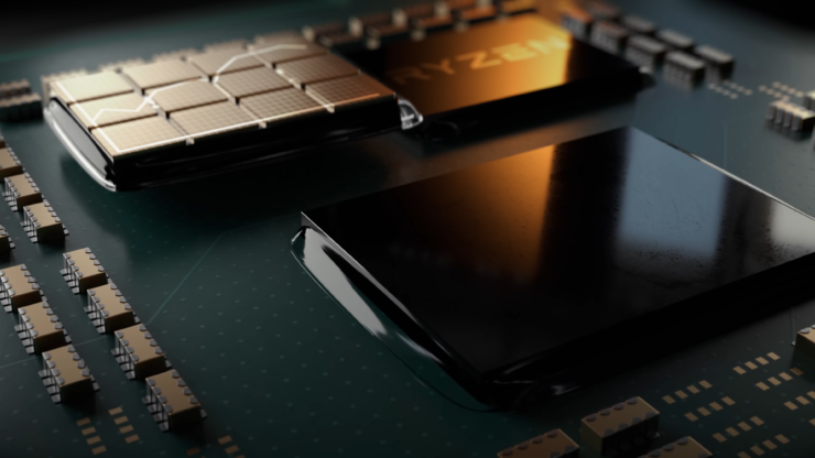
As the semiconductor industry ventures into the new era of “multi-chiplet” technology, breakthrough research has unveiled a fascinating solution for chipset interconnection through the use of silicon photonics, particularly optical interposers. This innovation could significantly impact the adoption of multi-chiplet designs, propelling advancements in the chip sector.
The escalating competition for chiplet designs in the CPU and GPU markets focuses on creating power-efficient solutions using this innovative technique. For those not familiar with the term, a chiplet is essentially an assembly of various chips combined into a single unit, linked through an interconnected system. This approach contributes to the overarching goal of “process shrinking.”
Chiplets can be composed of identical core IPs or various ones, offering a flexible mix-and-match strategy to optimize performance for specific product segments. Nonetheless, a critical aspect of this process is finding an effective interconnect method. A promising answer to this challenge, according to European technology research institute CEA-Leti, lies in leveraging silicon photonics via optical interposers—particularly the Starac interposers.
These optical interposers employ silicon photonics over traditional methods, merging electronic and photonic circuitry in one package for intricate data routing and processing. Moreover, the system includes a specialized Optical Network-on-Chip (ONoC), designed for speedy data transmission between chiplets, bypassing intermediate hops through a ring topology configuration.
Although Starac hasn’t been deployed yet, CEA-Leti expresses confidence that the technology will significantly lower latency, enhance bandwidth, and drastically elevate power efficiency, fostering widespread adoption by mainstream industry players. The company is currently seeking collaborations to put this concept into practice, though complex manufacturing processes and associated costs pose obstacles.
In the context of powerful computing systems, numerous compute chiplets with cores and HBMs (high-bandwidth memories) are employed. As observed with processors from major players like Intel, AMD, and Nvidia, data transfer from a core to a nearby HBM is straightforward. However, accessing more distant HBMs requires numerous operations to retrieve the data. The proposed solution aims to minimize latency, with light transmission within the optical network-on-chip offering intrinsic low latency compared to conventional architecture’s multiple hops.
Jean Charbonnier, R&D project leader at CEA-Leti, emphasizes the hope to establish industrial partnerships soon, which would help tackle process and packaging challenges and address real-world problems this technology could resolve.
Considerations around these innovations lead us to ponder whether Moore’s Law should be the sole guiding principle for advancements in computing, or if alternate avenues hold the key to future progress. In recent times, companies like NVIDIA have challenged Moore’s Law, highlighting the potential of focusing on other vital factors beyond process shrinking for technological evolution.
These promising developments illustrate the dynamic nature of the semiconductor industry and its potential to redefine computing landscapes through novel solutions like active optical interposers.