NVIDIA Pushes Next-Generation AI Networking With Optics-on-Interposer and DWDM Fiber Technology
NVIDIA is moving closer to a major shift in how future AI chips communicate, and the company’s latest research points to faster, denser, and more power-efficient optical connectivity for next-generation data centers.
As artificial intelligence models grow larger and AI factories demand more compute power, traditional electrical interconnects are becoming harder to scale efficiently. Moving massive amounts of data between GPUs, memory, switches, and accelerators requires enormous bandwidth, and that bandwidth must arrive with lower latency and reduced power draw. This is where co-packaged optics, often called CPO, is becoming increasingly important.
At SEMICON West 2026, NVIDIA presented new details on its work in advanced optical integration for future AI systems. The company discussed how co-packaged optics and dense wavelength-division multiplexing, or DWDM, could help solve some of the toughest connectivity challenges facing large-scale AI infrastructure.
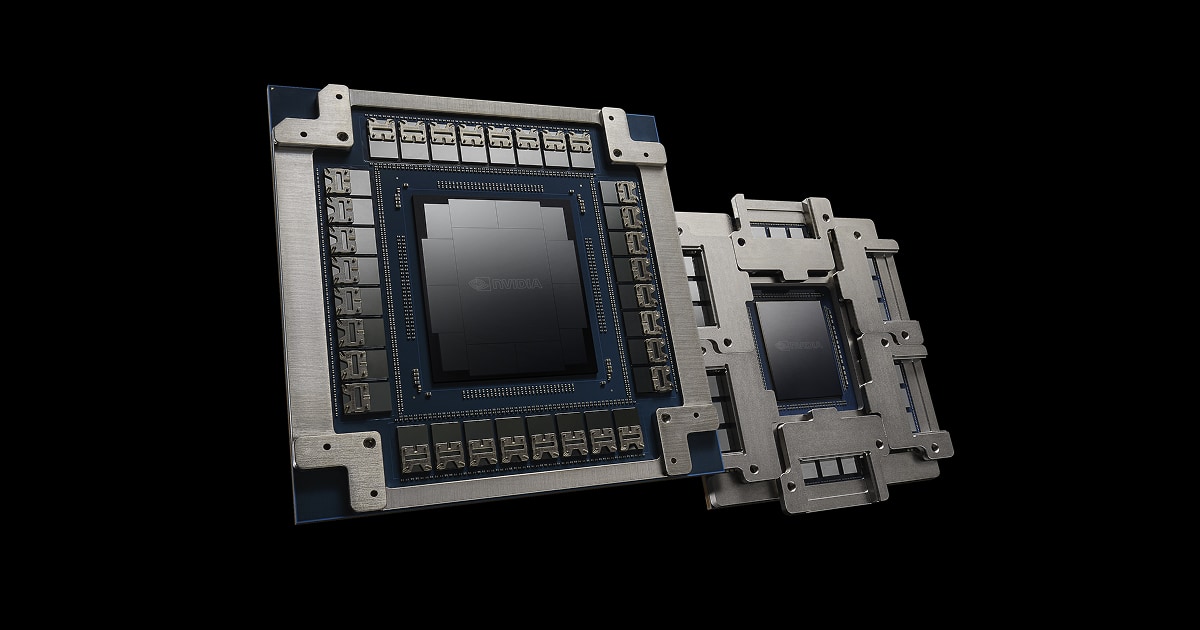
One of the biggest developments is NVIDIA’s prototype work on a technology it calls Optics-on-Interposer, or OOI. This approach takes optical engines that would traditionally sit on an organic substrate and moves them onto the silicon interposer. That may sound like a small packaging change, but it could have a major impact on future chip design.
By placing optical engines closer to the silicon interposer, NVIDIA can shorten the electrical signaling path and make use of finer-pitch, higher-density interconnects. In practical terms, this could mean higher bandwidth density, improved energy efficiency, and better scaling for future AI accelerators.
The idea is similar to how modern high-performance processors place GPUs and HBM memory extremely close together to maximize bandwidth and reduce power loss. Instead of sending signals across longer paths on a substrate, NVIDIA’s OOI concept brings critical optical communication components closer to the compute engine itself.
This could be especially important as AI platforms continue to scale beyond today’s systems. Future data centers will rely on thousands, and potentially tens of thousands, of accelerators working together. The faster those chips can exchange data, the more efficiently they can train and run large AI models.
NVIDIA is also working on DWDM technology, another key part of its future optical strategy. Dense wavelength-division multiplexing allows multiple wavelengths of light to travel through a single optical fiber path, increasing the amount of data that can be carried without requiring additional fibers.
In NVIDIA’s demonstration, eight wavelengths reached speeds of up to 32 Gb/s each, producing a combined 256 Gb/s of bandwidth over a single optical fiber path. While this technology remains in the research stage, it shows how NVIDIA is exploring ways to dramatically increase optical bandwidth for future AI networks.
Nikola Nedovic, NVIDIA’s Principal Research Scientist, has been one of the key figures behind this work. He previously outlined the motivation for bringing optics onto the silicon interposer, and NVIDIA’s latest prototypes suggest the company is making real progress toward that goal. According to Nedovic, the company is evaluating technologies intended for future products while also tackling the engineering barriers that still stand in the way of commercialization.
The timing is important. NVIDIA is already building a broad ecosystem around co-packaged optics for its AI platforms. Products such as BlueField-5, NVLink 8 CPO, Spectrum 7 204T CPO, and CX10 are part of the company’s wider plan to improve AI networking from the chip level to the full data center scale.
Looking further ahead, NVIDIA’s Feynman GPUs, expected around 2028, are likely to advance the company’s co-packaged optics roadmap even further. These future GPUs are expected to build on the Rubin Ultra generation and push optical integration deeper into NVIDIA’s AI hardware strategy.
The broader supply chain also appears to be preparing for this transition. Recent industry comments from major optical component suppliers indicate that demand for ultra-high-power CPO lasers is rising. Scale-out revenue is expected to begin in the second half of 2026, followed by scale-up volumes in 2027 and wider customer deployments in 2028.
This schedule aligns closely with NVIDIA’s future AI platform roadmap. As the company invests heavily in optical capacity and research, co-packaged optics could become one of the core technologies powering the next generation of AI factories.
The shift from conventional chip packaging to optical integration on the interposer will not happen overnight. There are still challenges in manufacturing, thermal management, reliability, cost, and large-scale deployment. However, NVIDIA’s prototype work shows that the company is actively preparing for a future where optical communication is no longer just a board-level or rack-level technology, but something integrated much closer to the processor itself.
For AI data centers, the benefits could be significant. Higher bandwidth density would allow more data to move between accelerators. Lower power consumption would help reduce one of the biggest operating costs in modern AI infrastructure. Better scalability would make it easier to build larger systems capable of handling increasingly complex AI workloads.
NVIDIA’s Optics-on-Interposer and DWDM research highlights a clear direction for the future of AI hardware: compute, memory, and networking are becoming more tightly integrated than ever. As AI systems expand in size and complexity, optical connectivity may become just as important as GPU performance itself.
If NVIDIA’s roadmap stays on track, co-packaged optics and advanced optical interposer designs could play a central role in the AI platforms arriving from Vera Rubin onward, with even more advanced implementations expected by the Feynman generation in 2028.