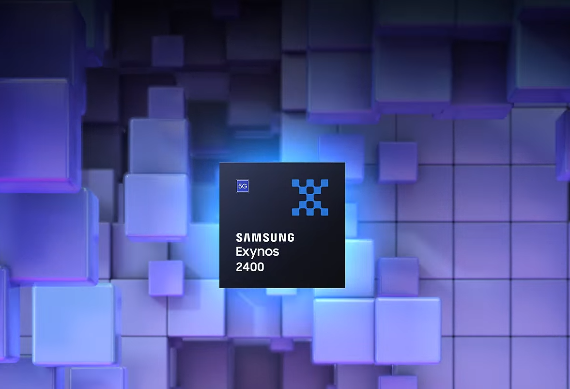
Samsung has recently unveiled the specifics of its much-anticipated Exynos 2400 chipset, confirming the integration of a deca-core CPU and Full-Scene Anti-Aliasing (FSR) support for its Xclipse 940 GPU. Initially announced with minimal detail and absent from the spotlight at the Galaxy Unpacked event, the Exynos 2400 spec sheet has now been officially updated on Samsung’s website.
At the heart of the new mobile SoC is a deca-core CPU comprised of various ARM Cortex cores. Leading the pack is a prime Cortex-X4 core clocked at 3.20 GHz, followed by a duo of Cortex-A720 cores at 3.9 GHz, enhanced by a triplet of Cortex-A720 cores at 2.60 GHz, and capped off by four Cortex-A520 cores at 2.0 GHz, arranged in a custom 1+2+3+4 configuration. The Exynos 2400 is a trailblazer as the first chip to leverage Samsung Foundry’s advanced 4LPP+ process and the innovative FOWLP (Fan Out Wafer Level Packaging) technology, promising superior energy efficiency over previous models.
In the graphics department, the Samsung Exynos 2400 will include the Xclipse 940 GPU, derived from AMD’s RDNA 3 architecture, an unprecedented move for a mobile SoC. This cutting-edge GPU is engineered to support hardware-accelerated ray tracing and variable rate shading techniques. Additionally, the Xclipse 940 is equipped with AI-driven upscaling capabilities akin to AMD’s FidelityFX Super Resolution, making it a future-forward choice for mobile graphics.
Despite Samsung not disclosing complete GPU specs, such as Work Group Processor (WGP) count and clock speeds (speculated in leaks to be about 1.1 GHz), the tech giant boasts that the Exynos 2400 is capable of delivering 4K resolutions at 120 frames per second (FPS) or 1440p resolutions at 144 Hz when connected to an external display.
Another significant leap forward for the Exynos 2400 is its Neural Processing Unit (NPU), which is touted to be more than fourteen times faster than its predecessor, the Exynos 2200. This is achieved through a blend of two General NPUs (GNPUs) and two Shallow NPUs (SNPUs), though precise TOPS performance metrics remain unspecified.
The Image Signal Processor (ISP) of the Exynos 2400 is designed to support massive camera sensors up to 320 megapixels, setting a new benchmark for mobile photography capabilities.
Samsung has confirmed that the international variants of the upcoming Galaxy S24 and Galaxy S24+ will be powered by the Exynos 2400 chipset, with the exception of the US, China, Canada, and Japan markets.
Samsung’s move to advance its Exynos line with state-of-the-art features reflects the company’s commitment to delivering high-performance, energy-efficient, and competitive mobile processors. The Exynos 2400, with its robust CPU and GPU coupled with advanced AI and ISP capabilities, is poised to be a potent force in next-generation Samsung Galaxy devices.
Anil Ganti, a Senior Tech Writer with extensive experience in covering the tech industry and a passion that has roots in PC gaming, brings this latest information on the Exynos 2400 SoC. With 1656 articles published on Notebookcheck since 2019 and a background in mechanical engineering, Anil offers valuable insights into the latest technological advancements.