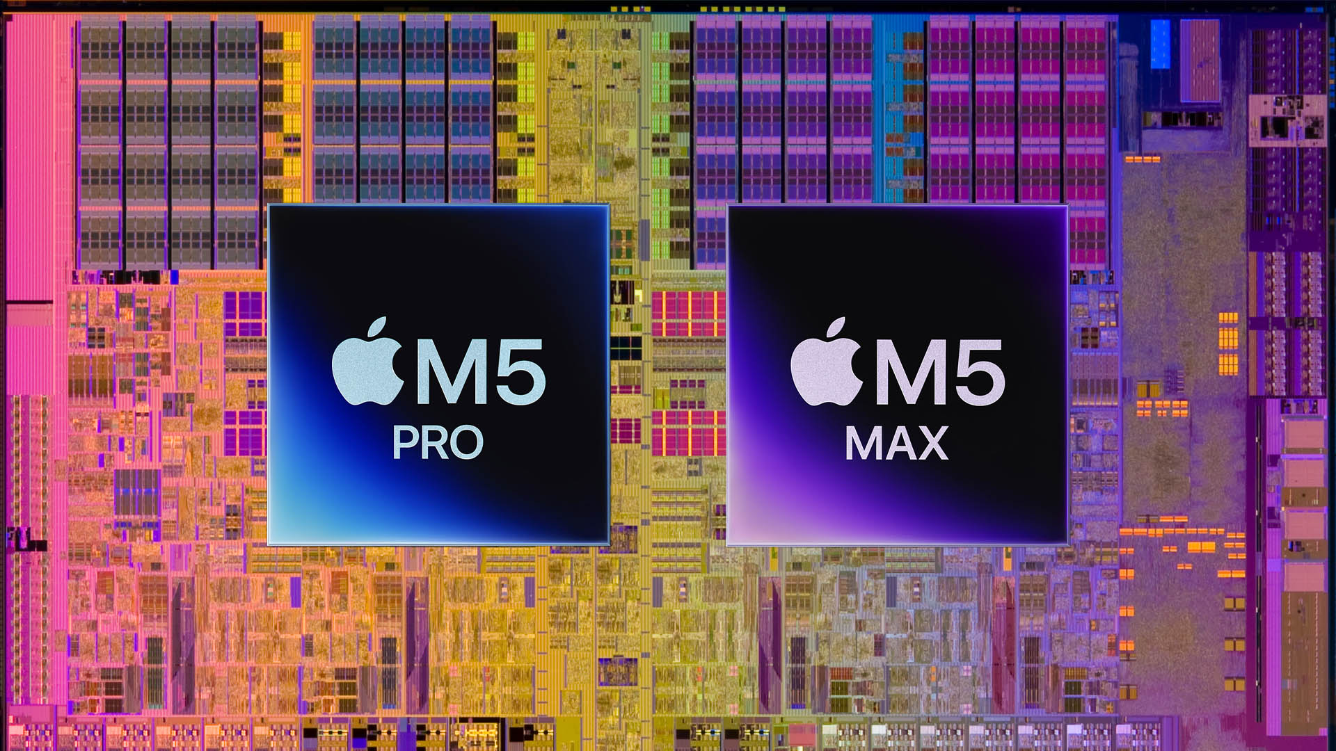
Apple is shaking up its Apple Silicon playbook with a new approach it calls “Fusion Architecture,” first introduced alongside the M5 Pro and M5 Max. The big headline is that these chips are said to move beyond the monolithic designs used in earlier generations, adopting a more advanced chiplet-style layout aimed at boosting performance, efficiency, and internal bandwidth.
In most modern chiplet approaches, different functional blocks live in separate regions or separate pieces of silicon, often connected through advanced packaging. What’s surprising here is a claim that the M5 Pro and M5 Max don’t just split functions across dies in a traditional 2.5D-style arrangement, but instead use vertically stacked dies. If accurate, that would mark a notable shift in how Apple is packaging its high-end laptop and desktop processors.
The discussion comes from an interview with Anand Shimpi, who works at Apple in its Hardware Technologies organization. In the interview, he explains that Apple’s earlier work on UltraFusion—in processors like the M2 Ultra and M3 Ultra—helped pave the way for this next step. But unlike the Ultra chips, which effectively paired two matching SoCs to create a bigger one, Fusion Architecture is described as splitting functions across two different dies that are not mirror images of each other. In other words, instead of duplicating the same silicon twice, Apple is reportedly distributing different IP blocks across separate dies to build the final processor.
If the “stacked dies” detail holds up, it suggests Apple is chasing faster die-to-die communication with lower latency and strong power efficiency—benefits typically associated with tighter physical proximity and higher-bandwidth connections between blocks like CPU, GPU, and other processing engines. This kind of packaging can, in theory, help Apple scale performance without relying solely on bigger single dies, which can be more complex and expensive to manufacture.
There is usually a trade-off with vertical stacking: heat. Sandwiching active components can raise thermal density, making cooling more challenging depending on what exactly is stacked and how the heat is spread through the package. That’s why one recent detail stands out: in a prior multi-core stress test, the M5 Max reportedly ran at lower temperatures than the M4 Max. If both reports are true, it could indicate Apple has made meaningful improvements in thermal design, power management, packaging materials, or the division of workloads across the dies.
That said, it’s worth being cautious. There’s some dispute about how the stacked-die comment should be interpreted, and even about Shimpi’s precise role. Because of those uncertainties—and because true confirmation typically comes from die shots and deeper technical teardowns—it’s best to treat the stacked-die claim as unconfirmed for now.
What’s clear is that Apple is continuing to evolve Apple Silicon at the packaging level, not just through CPU and GPU core updates. If Fusion Architecture really does introduce a new multi-die, potentially stacked design to the M5 Pro and M5 Max, it could be a key reason these chips deliver stronger performance per watt, better scaling at the high end, and improved efficiency in real-world workloads. As more technical evidence appears, we should get a clearer picture of how Apple’s next-generation chip design is actually built.