Samsung’s M2800 5G Modem Could Mark a Major Shift to 2nm Manufacturing
Samsung appears to be preparing a significant change in its semiconductor strategy, with its upcoming M2800 5G modem expected to move from the company’s 4nm process to its more advanced 2nm node. If this transition happens as reported, it would represent the first major lithography upgrade for Samsung’s baseband chip lineup and could become an important turning point for its foundry business.
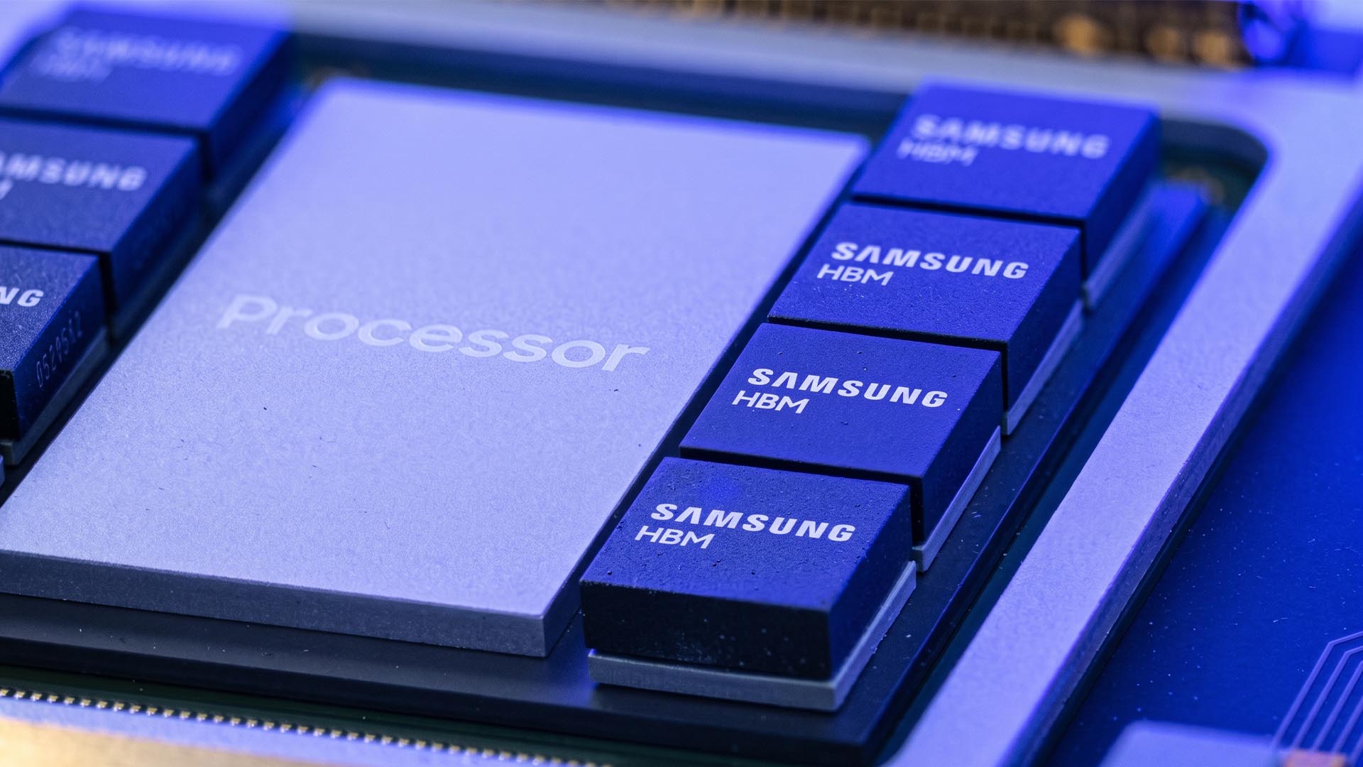
The shift is not happening in isolation. Samsung has reportedly been reorganizing its manufacturing resources as demand grows for HBM, or high-bandwidth memory, which is becoming increasingly important for AI accelerators, data centers, and next-generation computing hardware. By accelerating development of HBM base dies on its 4nm process, Samsung may now have more room to explore 2nm production for other advanced components, including the M2800 5G modem.
This could give Samsung a valuable opportunity to strengthen its position against TSMC, especially as the race for advanced chip manufacturing becomes more competitive.
Why Samsung’s 2nm Move Matters
For years, Samsung has faced challenges in winning major foundry orders for advanced mobile chips, partly due to concerns over yields and manufacturing efficiency. Moving the M2800 modem to 2nm could help the company demonstrate that its latest process is maturing and ready for more demanding semiconductor products.
The M2800 5G modem is expected to be an important piece of Samsung’s next-generation mobile hardware strategy. A smaller, more advanced manufacturing process can potentially improve power efficiency, thermal performance, and overall modem capability. In smartphones, where battery life and connectivity performance are crucial, these improvements could matter a great deal.
A successful 2nm modem would also show that Samsung is not limiting its newest node to flagship application processors alone. Alongside chips such as the expected Exynos 2700, the M2800 could help increase Samsung’s 2nm utilization, which is essential for improving production efficiency and reducing manufacturing costs over time.
HBM Production Could Be the Key
One of the most interesting parts of Samsung’s strategy is how HBM production fits into the larger foundry picture. Samsung has reportedly focused heavily on producing HBM base dies using its 4nm process. This is important because HBM4 and future memory technologies require strong performance, fast lane speeds, and efficient design.
Using a more advanced node for HBM base dies could help Samsung avoid performance limitations associated with older manufacturing processes. In comparison, some competing HBM-related production has relied on less advanced nodes, which may create bottlenecks as bandwidth demands increase.
By dedicating 4nm capacity to HBM base dies, Samsung may be able to free up its most advanced 2nm resources for products like the M2800 modem. This creates a two-part advantage: the company strengthens its HBM position while also giving its next-generation modem technology a chance to evolve on a more advanced manufacturing process.
Qualcomm Could Be Watching Closely
Samsung’s progress on 2nm manufacturing could also have major implications for Qualcomm. The two companies have had a complicated foundry relationship in recent years, with Qualcomm often relying heavily on TSMC for its most advanced Snapdragon chips.
That strategy has delivered strong performance, but it also comes at a high cost. TSMC’s leading-edge nodes are in high demand, especially as Apple, Nvidia, AMD, and other major chip designers compete for capacity. For Qualcomm, depending on a single foundry can be expensive and strategically limiting.
If Samsung can prove that its 2nm process is reliable, efficient, and cost-competitive, Qualcomm may have a stronger reason to consider a dual-foundry approach. Splitting production between TSMC and Samsung could help Qualcomm negotiate better pricing, reduce supply risk, and improve flexibility for future Snapdragon platforms.
Samsung may also be in a position to offer more attractive pricing as 2nm utilization improves. Higher usage of a manufacturing node usually helps lower costs over time, and products like the Exynos 2700 and M2800 modem could be important in reaching that point.
A Potential Foundry Comeback for Samsung
Samsung has been working to regain momentum in the advanced foundry market, where TSMC currently holds a dominant position. The move to 2nm modem development could become part of a broader comeback effort, especially if the company can combine improved yields, competitive pricing, and strong performance.
The M2800 5G modem may not be as publicly visible as a flagship smartphone processor, but it could play a meaningful role in proving Samsung’s 2nm capabilities. Modems are complex, power-sensitive components, and successful production on a cutting-edge node would send a strong signal to potential customers.
At the same time, Samsung’s focus on HBM base dies could help it capitalize on the explosive demand for AI memory hardware. If the company can execute well in both HBM and 2nm logic manufacturing, it may strengthen its position across two of the semiconductor industry’s most important growth areas.
The Bigger Picture
Samsung’s reported move from 4nm to 2nm for the M2800 5G modem is more than a routine process upgrade. It reflects a larger strategy involving HBM production, foundry utilization, cost competitiveness, and future customer wins.
If Samsung succeeds, the benefits could extend beyond its own Exynos ecosystem. Qualcomm could gain a stronger alternative to TSMC, Samsung could improve its foundry reputation, and the mobile chip market could become more competitive.
For now, the M2800 5G modem is shaping up to be a key product to watch. Its success could help determine whether Samsung’s 2nm technology becomes a serious option for major semiconductor customers in the years ahead.