Good news is emerging from Intel’s camp as its 18A process is reportedly achieving impressive yield rates, currently surpassing some competitors.
Intel’s 18A Yield Rates Show Promise for Mass Production by Late 2025 with Panther Lake SoCs
Despite the lack of full disclosure on specific yield rate figures, recent insights from KeyBanc Capital Markets suggest Intel’s 18A node is advancing swiftly in development. While it outpaces Samsung’s SF2, it remains slightly behind TSMC’s N2. Nonetheless, this progress indicates that Intel is on track for high-volume manufacturing by year’s end.
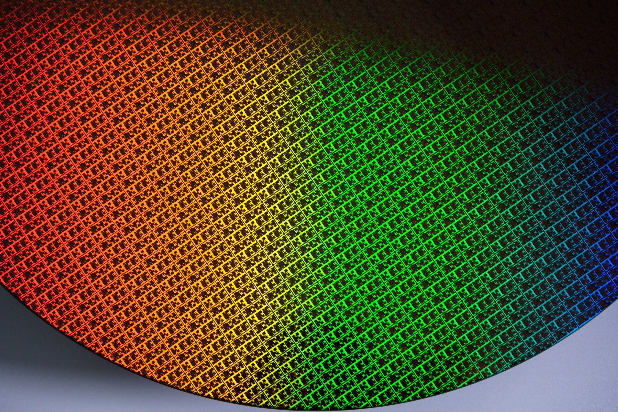
Intel’s 18A process has seen a yield rate boost, now at 55%, up from 50% last quarter. In comparison, Samsung’s 2nm process (SF2) is estimated around 40%, while TSMC’s N2 leads with 65%.
Improving yield rates is vital for Intel as the 18A is primarily focused on internal products like Panther Lake. Achieving strong results at this stage is crucial. KeyBanc highlights that Intel aims to mass-produce 18A for next-gen mobile CPUs, with yields projected to reach 70% by Q4 2025. While not surpassing TSMC’s rates, having a robust node is essential for Intel’s competitive edge.
There has been speculation about the future success of Intel’s 18A node. However, its effective use internally could deem this process successful. Intel seeks to gain traction in cutting-edge technology with 18A, planning to transition to external clients with 14A. This strategy may help them introduce a strong product to the market, potentially challenging TSMC’s A14. Much anticipation surrounds the Panther Lake’s consumer market performance, given the optimism based on past observations.