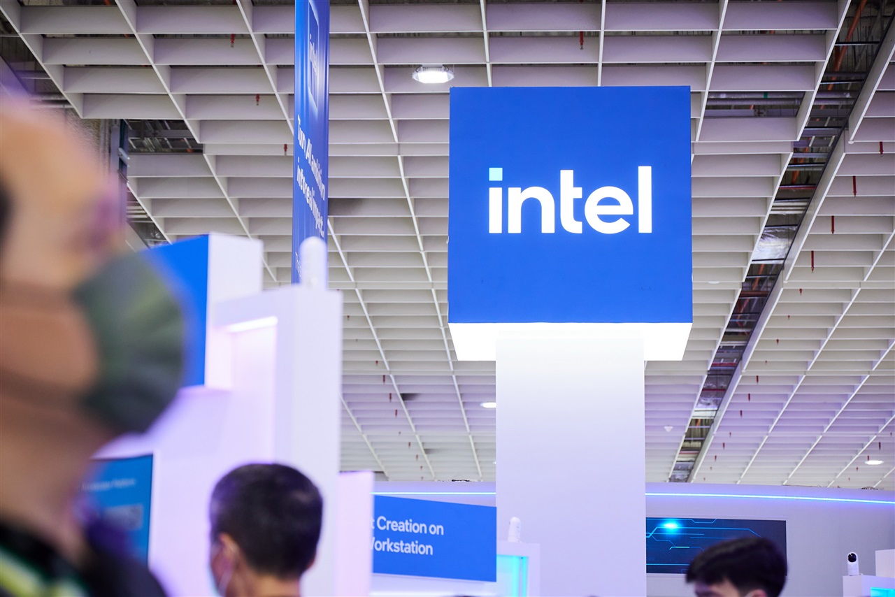
Intel’s AI chip strategy is getting a bold reboot. The long-teased Falcon Shores accelerator is effectively sidelined, and a new platform called Jaguar Shores is taking the lead. Early test photos are already circulating, and at the company’s AI Summit in July 2025, Intel confirmed Jaguar Shores will integrate SK Hynix’s next-generation HBM4 memory. More than a single chip, Jaguar Shores is being framed as a flagship, rack-scale AI system designed to go head-to-head with Nvidia and AMD as the industry transitions to HBM4-based accelerators through 2026.
HBM4 is the battleground. Nvidia is reportedly preparing to bring parts of HBM manufacturing in-house around 2027, a move that could change supplier dynamics. Yet analysts believe SK Hynix will remain pivotal thanks to its scale and track record, even as chipmakers push for customized HBM stacks to squeeze out more bandwidth, lower latency, and better power efficiency. That shift will likely tighten collaboration between compute and memory teams on both sides, blurring the traditional line between chip designers and memory vendors.
Another twist in the race to 2nm: Samsung is said to be weighing a strategic investment in Intel. The reported goal is to tap into Intel’s strengths in advanced packaging—think hybrid bonding and glass substrates—to give Samsung’s foundry efforts more firepower and sharpen competition with TSMC. The timing is notable as Samsung expands its US footprint with a multibillion-dollar fab in Texas and as political headlines swirl following a disclosure that Washington now holds nearly 10% of Intel. With Samsung targeting 2nm and Intel pushing its 18A process, a closer alliance on packaging and cost controls could reshape pricing and accelerate adoption of cutting-edge nodes for consumers and enterprises alike.
Samsung’s memory ambitions are also in the spotlight. During South Korea’s high-profile US outreach—anchored by a US$150 billion pledge spanning chips, shipbuilding, and AI—semiconductors took center stage. At the KORUS Business Roundtable in Washington, a candid moment between Samsung chairman Jay Y. Lee and Nvidia CEO Jensen Huang captured attention, underscoring how pivotal Nvidia’s HBM4 supplier choices will be. Samsung’s HBM4 samples are due by late August, and winning that socket could recalibrate the company’s memory trajectory for years to come. South Korean leaders emphasized that high-bandwidth memory is foundational to US AI competitiveness, with Samsung and SK Hynix set to expand their American manufacturing footprint.
The momentum isn’t confined to the US and Korea. In India, consumer electronics brand boAt and semiconductor startup HrdWyr unveiled the Indus 1011, a fully India-designed chip backed by Tata Electronics for assembly, packaging, and testing. Targeted for boAt’s next-gen premium wireless charging cases in early 2026, the Indus 1011 showcases India’s push into low-power, AI-infused silicon while building domestic IP and back-end manufacturing depth. Analysts see the project as a proof point for the country’s “Make in India” and “Atmanirbhar Bharat” goals, potentially reducing reliance on foreign designs and supply chains.
Meanwhile, Micron is tightening its hold on Samsung’s flagship smartphone memory. After yield headwinds at Samsung’s own chip unit, Micron now supplies roughly 40% of the LPDDR5X for the Galaxy S25, according to industry chatter. A July meeting between Micron CEO Sanjay Mehrotra and Samsung mobile chief Roh Tae-moon signals that the partnership is likely to extend into the Galaxy S26 cycle. For Samsung’s handset arm, dual-sourcing adds resilience. For Micron, it cements stature as a strategic DRAM partner, even if margins stay tight and capacity remains carefully managed.
On the storage front, both Samsung and SK Hynix are dialing back spend on advanced NAND as the economics favor higher-margin DRAM and AI-centric packaging. Reports indicate Samsung has delayed ninth-generation NAND upgrades at Pyeongtaek and Xi’an and pushed out hybrid bonding adoption to at least 2026. SK Hynix is prioritizing DRAM and HBM for AI servers. Even so, there’s meaningful progress: SK Hynix just announced a 321-layer QLC NAND part that doubles capacity over its predecessor and delivers big gains in speed, efficiency, and density. It’s tuned for PCs and smartphones today, with an eye on ultra-high-capacity SSDs for AI servers as the ecosystem matures.
Global supply dynamics are being reshaped on another front: China’s AI hardware market is swerving toward second-hand Nvidia GPUs after Beijing’s ban on the H20 accelerator. Companies are sourcing used A100 and H100 units from overseas, repurposing them into inference servers to cut costs and dodge export constraints. Prices on used H100 systems have already fallen close to 25% this year, with steeper declines expected into 2026. The influx lowers barriers for AI developers and could accelerate adoption of inference at scale, but it also pressures domestic chipmakers and may introduce instability as gray-market hardware undercuts planned upgrade cycles.
Why this all matters:
– The next wave of AI accelerators will be defined by memory bandwidth, power efficiency, and packaging breakthroughs as much as by raw compute. HBM4 and advanced 2.5D/3D integration are the levers.
– Intel’s Jaguar Shores marks a strategic reset, betting on a rack-scale approach and tight memory integration to challenge entrenched incumbents.
– Foundry and packaging alliances are becoming as critical as process nodes. Closer Samsung–Intel cooperation could shift cost and technology roadmaps across the industry.
– India’s Indus 1011 highlights the democratization of chip design and advanced packaging, expanding the global talent and supply base for AI hardware.
– DRAM and HBM are soaking up capital as NAND investment cools, but breakthroughs like 321-layer QLC show storage innovation is far from stalling.
– Secondary markets for GPUs are rewriting the economics of AI buildouts in China, with ripple effects for pricing, supply chains, and regional competitiveness.
The world’s AI stack is moving fast toward 2nm-class nodes, HBM4, and sophisticated packaging that blurs the boundary between logic and memory. Expect deeper partnerships across compute and memory, more regionalized manufacturing, and a widening gap between those who master integration and those who only chase die shrinks. In that future, Jaguar Shores versus Nvidia’s next-generation platforms is just one storyline—the real race is about who can align design, memory, packaging, and supply at global scale.


